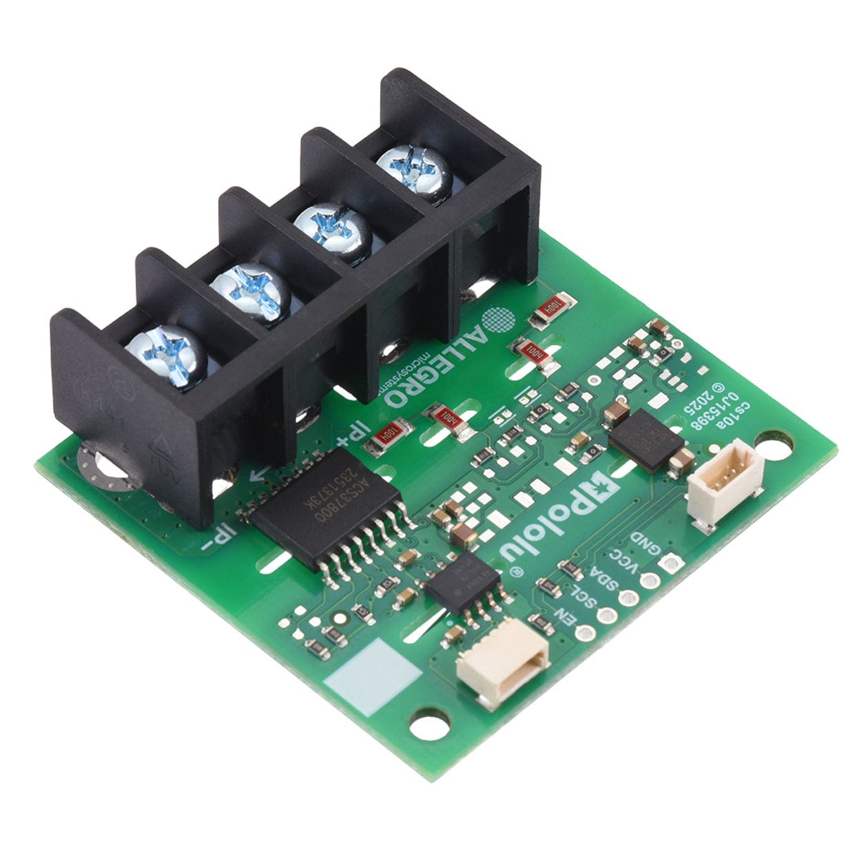
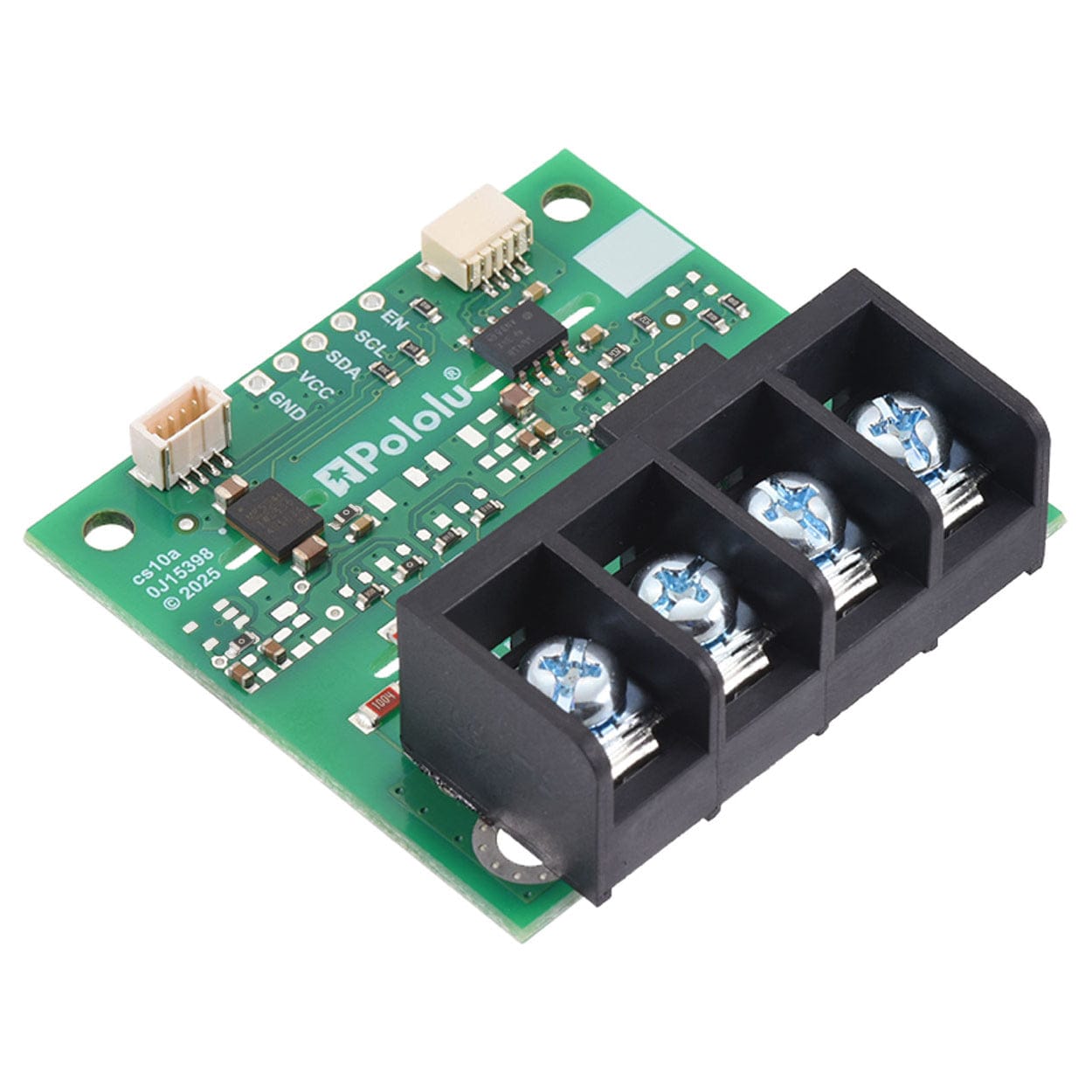
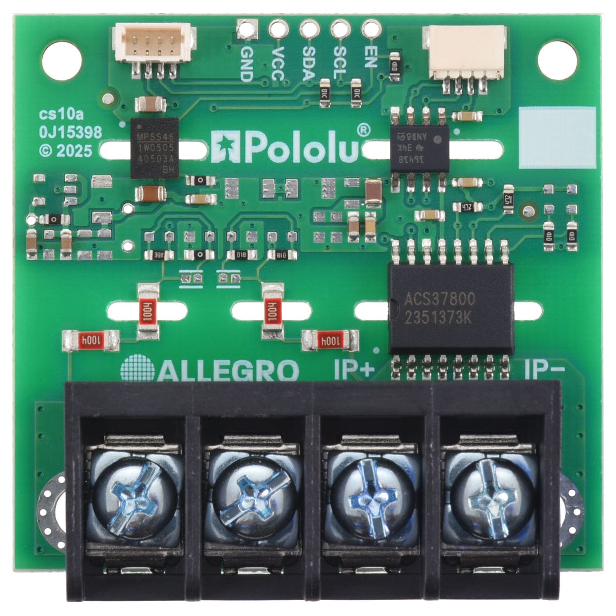
This board from Pololu is an integrated solution for monitoring voltage, current, power, and other parameters in AC and DC systems, featuring Allegro’s ACS37800KMACTR-030B3-I2C isolated power monitoring IC.
It provides bidirectional current measurements from −30 A to +30 A and can be configured to measure voltages up to 480 VRMS nominal (up to ±980 V peak). Our carrier board adds secondary isolation to the sensor’s I²C interface for additional safety and measurement accuracy. This version has a soldered Amphenol YK4410403000G terminal block rated up to 300V.
We are offering these breakout boards with support from Allegro Microsystems as an easy way to use or evaluate their ACS37800KMACTR-030B3-I2C isolated power monitoring IC; we therefore recommend careful reading of the ACS37800 datasheet before using this product.
This version of the ACS37800 power monitor carrier has a soldered terminal block (Amphenol YK4410403000G). We stock two versions of this board - one with no voltage measurement range set (defaults to 120VRMS) and one with jumpers pre-configured for 240VRMS. Please select an option before adding to cart.
Warning: This product is not designed to or certified for any particular high-voltage safety standard. Working with higher voltages can be extremely dangerous and should only be attempted by qualified individuals with appropriate equipment and experience.
Features
The following list details some of the sensor’s key features:
- Measures voltage and current, both RMS and instantaneous
- Works in single-phase AC and DC systems
- Automatic zero-crossing detection and averaging
- Calculates active, reactive, and apparent power, as well as power factor
- 1 kHz bandwidth
- Hall effect-based current sensor with an electrically isolated current path
- Sensor can be inserted anywhere along the current path
- Differential Hall sensing rejects errors from common-mode fields (e.g. Earth’s magnetic field)
- Low conductive path resistance (0.85 mΩ in ACS37800, PCB uses 2 oz copper)
- Board includes a resistor network with isolation and sense resistors for measuring voltage
- Three configurable voltage measurement ranges optimised for 120 VAC, 240 VAC, and 480 VAC measurement
- 1206-size, high-voltage-rated resistors on input voltage dividers
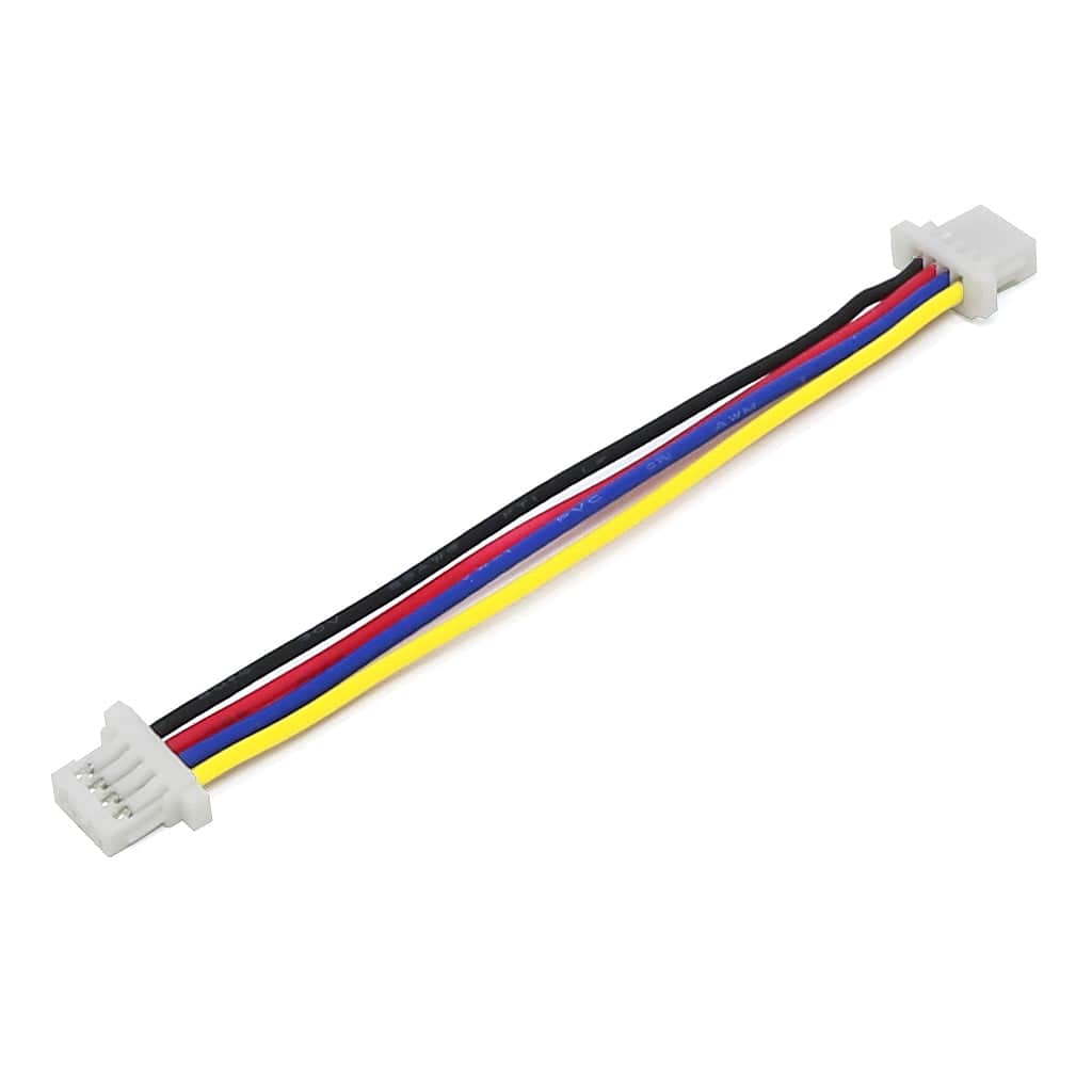
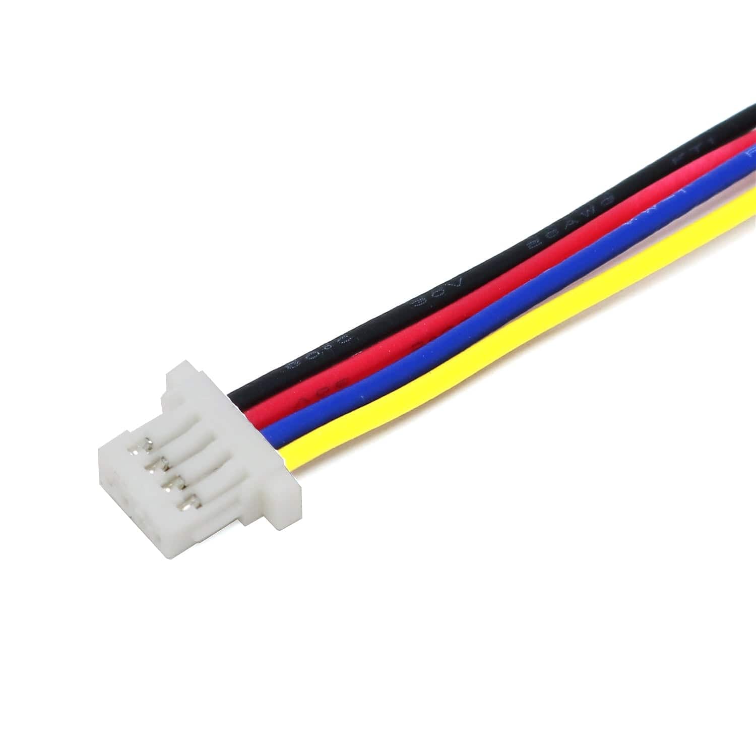
- Interface: I²C, using JST SH-style 4-pin connectors (Qwiic/STEMMA QT compatible) or 0.1″-pitch pins
- User configuration of the IC is stored in on-chip EEPROM
- Programmable over-current, under-voltage, and over-voltage detection thresholds
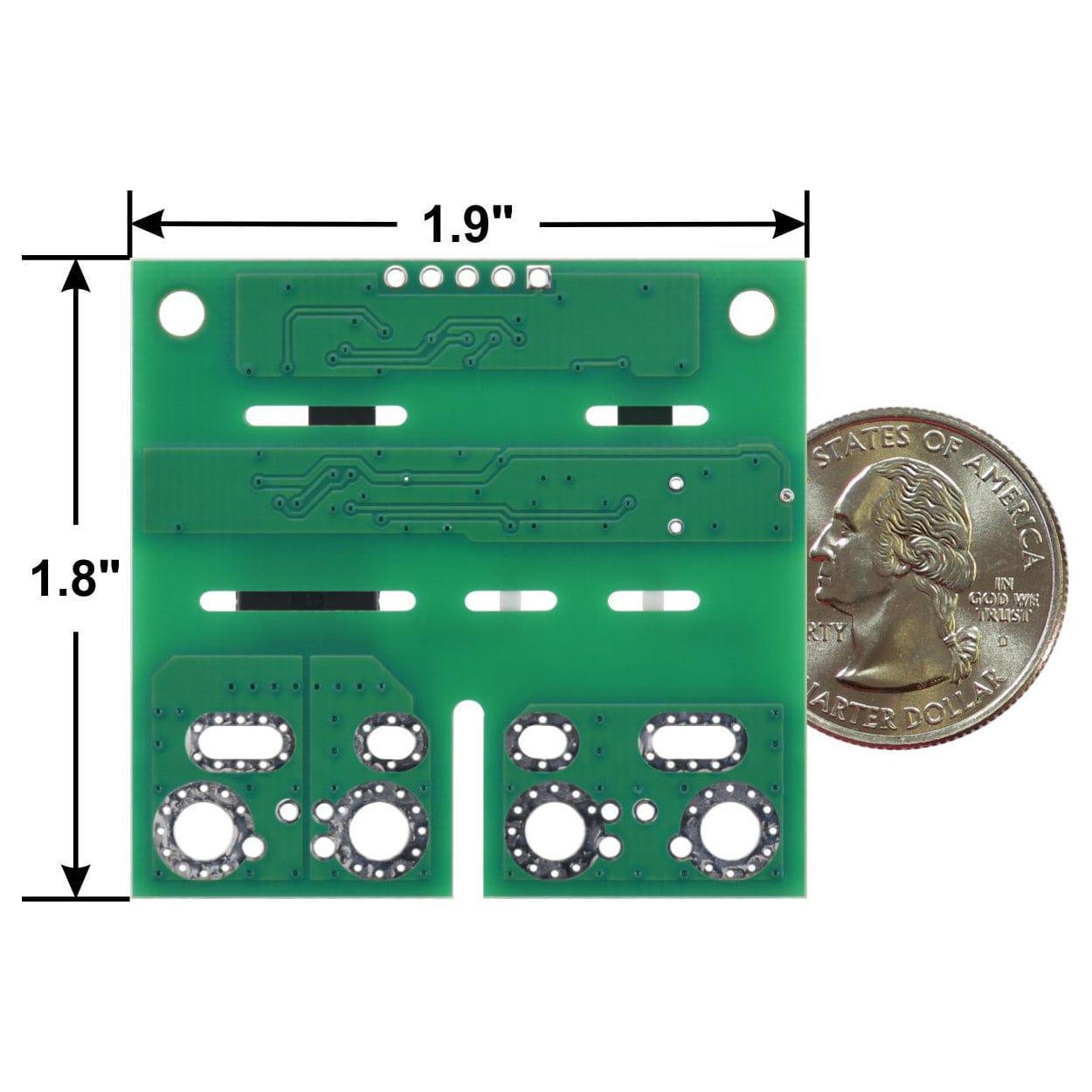
- Compact 1.9″ ×1.8″ board size
Using the sensor
The ACS37800 measures current flowing from the IP+ to the IP− connection points; these pins are labelled on the board’s top silkscreen, which also shows the direction that is interpreted as positive current flow via the +i arrow.
It measures voltage between IP+ and the connection points on the left side of the board (labelled V− in the schematic), with positive readings corresponding to a higher voltage on IP+. The left-side through-holes are all electrically connected, so one convenient way to make connections to the board is to attach your power supply to the inner set of connection points and your load to the outer set, as shown in the diagram below. (Alternatively, you can connect the negative sides of your load and power supply directly together, then add a separate connection from there to V−.)

When measuring DC systems, matching the polarities in this diagram will produce positive current readings when current flows from the power supply to the load and positive voltage readings when the supply has a higher voltage on its positive terminal than its negative terminal. In AC systems, the polarities are less important, though they might still be meaningful for the instantaneous voltage and current readings provided by the ACS37800.
On the logic side, the sensor has four required connections: logic power (VCC and GND) and I²C clock and data signals (SCL and SDA). These connections can be made through either of the board’s two JST SH-style 4-pin connectors, which work with our 4-pin JST SH-style cables and are compatible with SparkFun’s Qwiic and Adafruit’s STEMMA QT (the second connector can be used to chain additional I²C devices), or with a set of through-holes that are spaced with a 0.1″ (2.54 mm) pitch and compatible with 0.1″ male headers and solderless breadboards.

The carrier board configures the ACS37800 to use a 7-bit I²C target address of 0b1100000 (0x60 or 96) by default. However, the target address can be changed by reprogramming the EEPROM, as can many other configuration settings.
A logic supply voltage of 3 V to 5.5 V should be connected across VCC and GND. SCL and SDA are pulled up to this voltage, so VCC should match the logic level voltage of your I²C bus. VCC powers the ACS37800 through the on-board isolated DC-DC power module, which provides a regulated 3.3 V supply to the sensor, and the on-board I²C isolator also acts as a level shifter between the external I²C voltage level and the 3.3 V used by the sensor. This secondary layer of isolation makes it less likely for safety and measurement accuracy to be inadvertently compromised, such as if the board’s logic supply shares a ground with the system being measured.
An additional pin, EN, is brought out to the 0.1″-pitch through-holes. This is the enable input for the isolated power module and is pulled up to enable it by default. EN can be driven low to disable the board’s logic power and put it into a low-power state (note that the part of the circuit powered by VCC on the external side of the isolation barrier is not powered down).
You can make connections to the bare carrier board in a variety of ways. The largest through-holes are 4 mm in diameter with 12.5 mm spacing. These can be used with #6 or M3.5 screws for attaching various types of lugs or solderless ring terminals, or thick wires up to 10 AWG can be soldered directly to the board. The slots above the large through-holes can accommodate a 4-pin terminal block or other connector with a pitch between 9.5 mm and 12 mm.
This version of the board comes with a soldered terminal block, the Amphenol YK4410403000G, which is rated up to 300V. Holes with 0.1″ and 0.2″ (5 mm) spacing are also available for connecting male header pins or terminal blocks, but please note that these smaller connection options are generally not suitable for high currents like those this sensor is intended for.
Creepage and high voltage considerations
This product is not designed to or certified for any particular high-voltage safety standard. The PCB traces are laid out to provide at least 5 mm of creepage between the high-voltage input lines and 4 mm across each of the two high-voltage, 1206-size resistors that has an isolation slot routed under it. The secondary isolation to the I²C user interface also has creepage of greater than 4 mm. A rough rule of thumb is that uncontaminated FR4 PCBs should have approximately 1 mm of creepage per 100 VRMS of isolation.
Warning: This product is not designed to or certified for any particular high-voltage safety standard. Working with higher voltages can be extremely dangerous and should only be attempted by qualified individuals with appropriate equipment and experience.
Voltage measurement ranges
The carrier board has two surface-mount jumpers that can be used to configure one of three different voltage measurement ranges for the ACS37800.
These ranges are optimised for measuring 120 V, 240 V, and 480 VAC RMS (root mean square). To facilitate over-voltage detection, each range can handle an instantaneous voltage roughly 40% higher than the nominal peak voltage (or twice the nominal RMS voltage) before the sensor’s output saturates.

| Jumpers closed | Nominal VRMS range | Maximum VRMS | Maximum VPK or VDC | RSENSE |
| None | 120 VRMS | 170 VRMS | 245 V | 4 kΩ |
| Left | 240 VRMS | 345 VRMS | 490 V | 2 kΩ |
| Both | 480 VRMS | 690 VRMS | 980 V | 1 kΩ |
We stock two versions of the board (select an option before adding to cart).
- In the 120VRMS version, both jumpers are open, and the 120 VRMS range is selected by default
- The 240VRMS version has jumpers pre-configured for 240 VRMS
The board has two 1 MΩ isolation resistors in series between each voltage sensing terminal (IP+ and V−) and the corresponding sense input pin on the ACS37800 (VINP and VINN), for a total RISO of 4 MΩ. See the ACS37800 datasheet for details on converting the sensor’s raw readings into actual voltages based on RSENSE and RISO.
Real-world power dissipation considerations
The ACS37800KMACTR-030B3-I2C can measure up to ±30 A. In our tests, we found that our carrier board could conduct 30 A continuously without reaching the thermal limit for the IC. Our tests were conducted at approximately 25°C ambient temperature with no forced air flow.
The actual current you can pass through the sensor will depend on how well you can keep it cool. The carrier’s printed circuit board is designed to help with this by drawing heat out of the sensor chip. Solid connections to the current path pins (such as with thick soldered wires or large, tightly-secured lugs) can also help reduce heat build-up in the sensor and carrier board.
Warning: Exceeding temperature or current limits can cause permanent damage to the sensor. If you are measuring an average continuous current greater than 20 A, we strongly recommend that you monitor the sensor’s temperature and look into additional cooling if necessary.
Warning: This product can get hot enough to burn you long before the chip overheats. Take care when handling this product and other components connected to it.
Specifications
| Size | 1.8″ × 1.9″ × 0.78″ |
| Weight | 22 g |
| Minimum logic voltage | 3 V |
| Maximum logic voltage | 5.5 V |
| PCB dev codes | cs10a |
| Other PCB markings | 0J15398 |
Resources
Package Contents
- 1x Pololu ACS37800KMACTR-030B3-I2C Power Monitor Carrier with Secondary I²C Isolation (Soldered Terminal Block)
- Select 120VRMS or 240VRMS version before adding to cart