Pololu I²C Isolator with Connectors
Price:
Sale price
£5.60
Stock:
Quantity:
Login / Signup
Cart
Your cart is empty


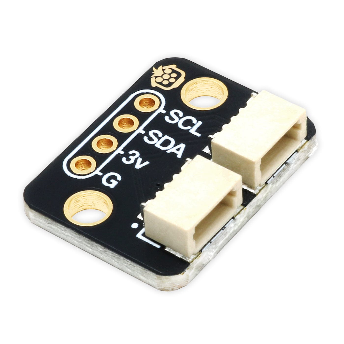
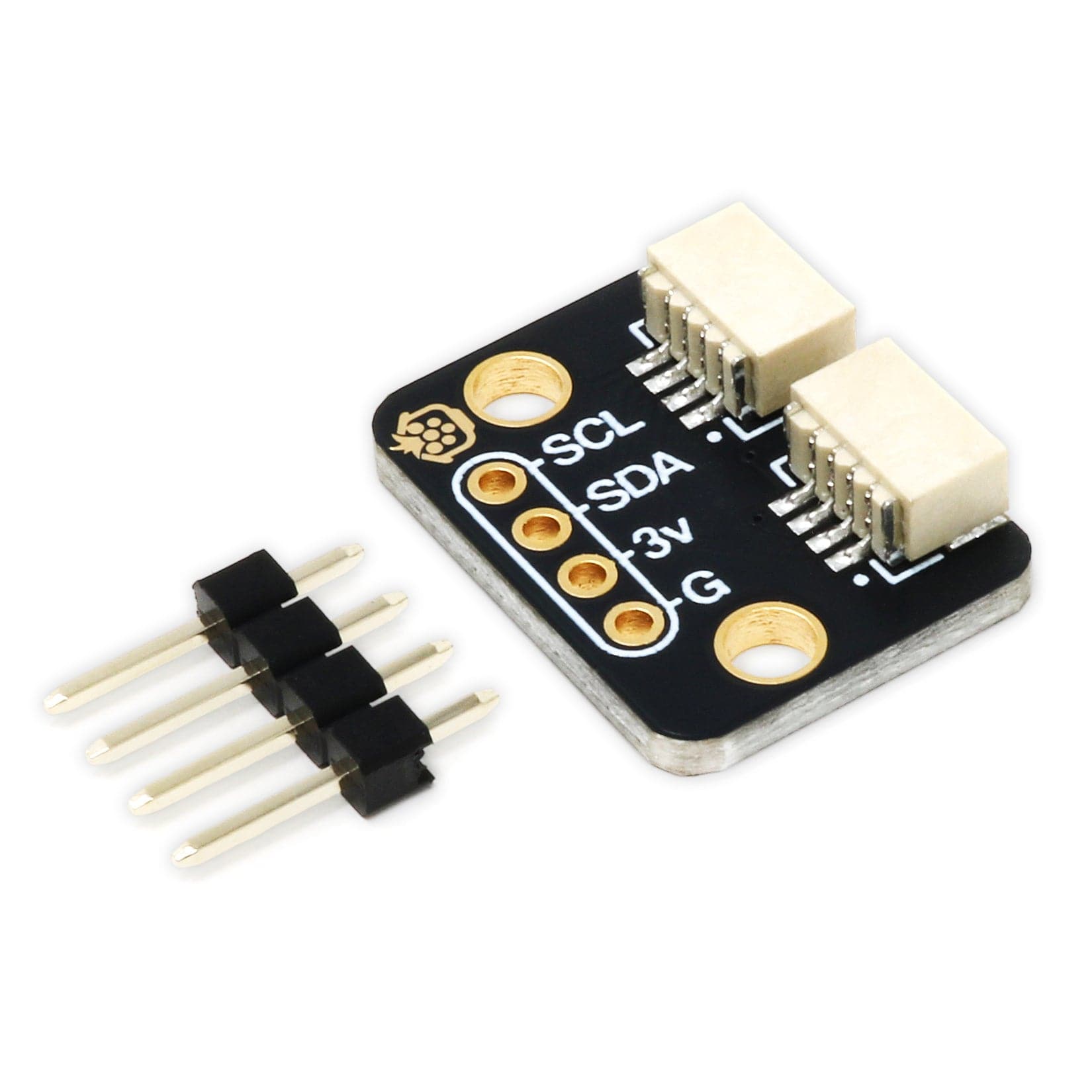
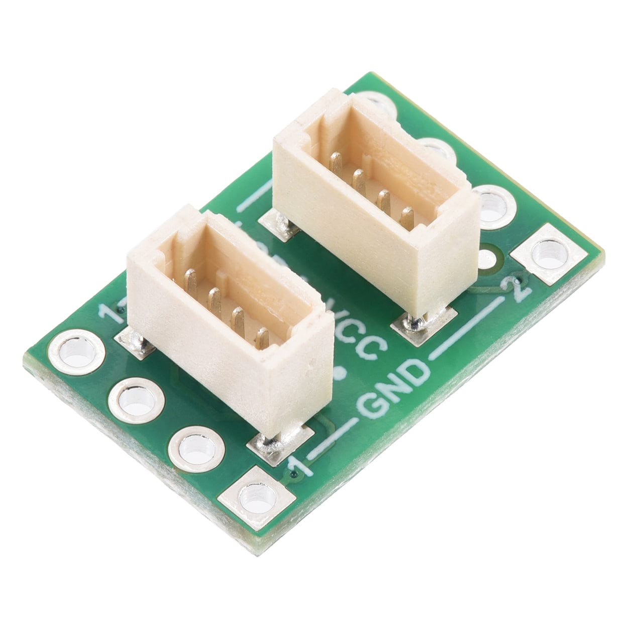
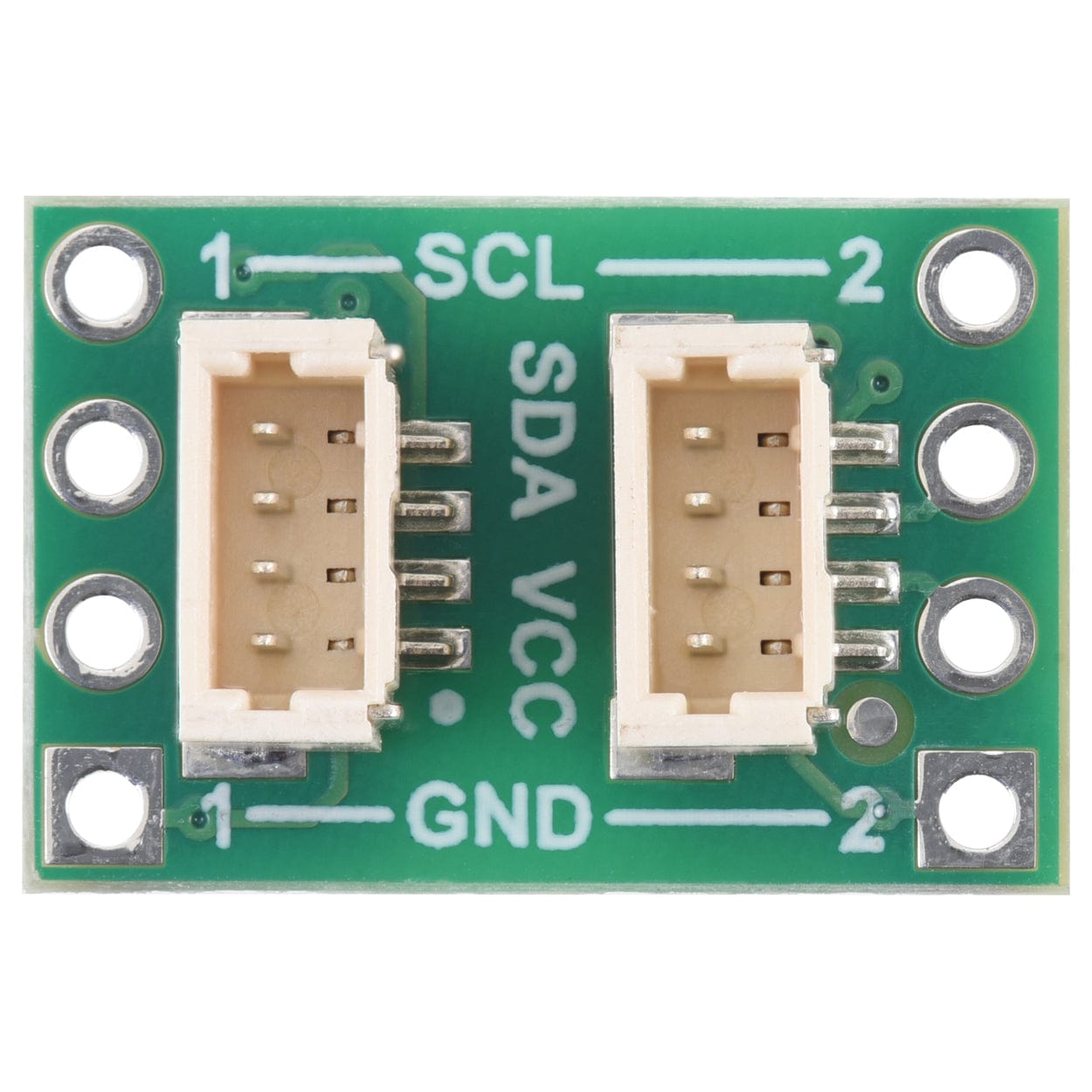
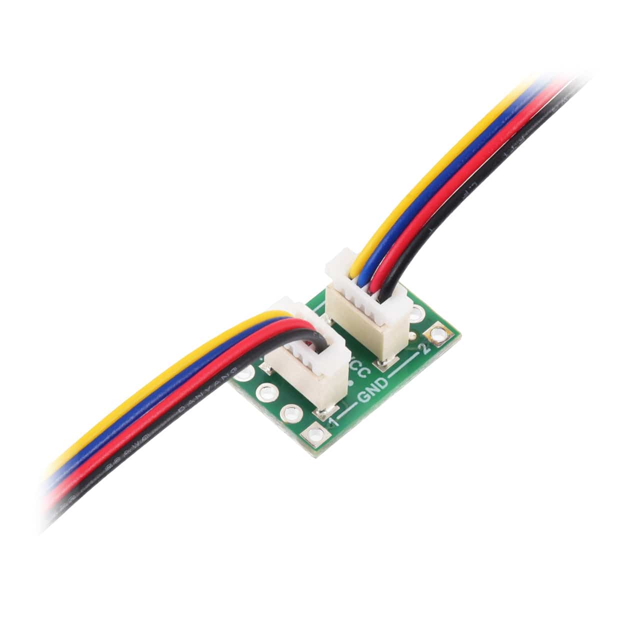
This Pololu module enables galvanically isolated (electrically isolated), bidirectional communication between two I²C devices, and comes with JST-SH (Qwiic/STEMMA QT compatible) connectors.
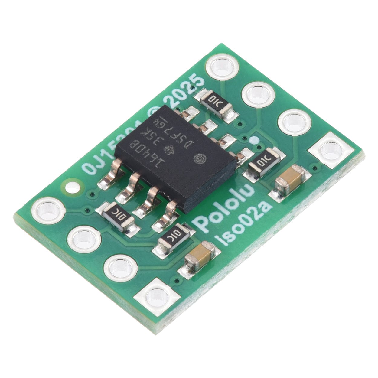
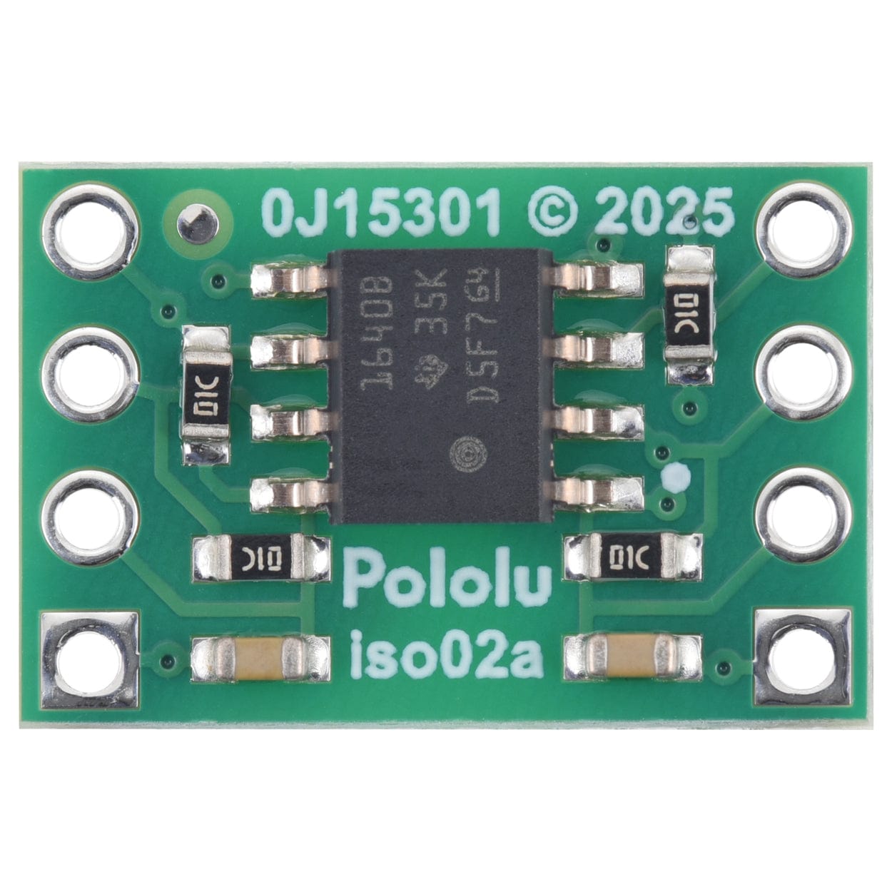
This isolation means current cannot flow from one side to the other, and incorrect connections or bad voltages on one side cannot propagate through to damage the device connected to other side. The module is based on the TI ISO1640B, which supports bidirectional data transfer up to 1.7 MHz. See the ISO1640BDR datasheet for more information.
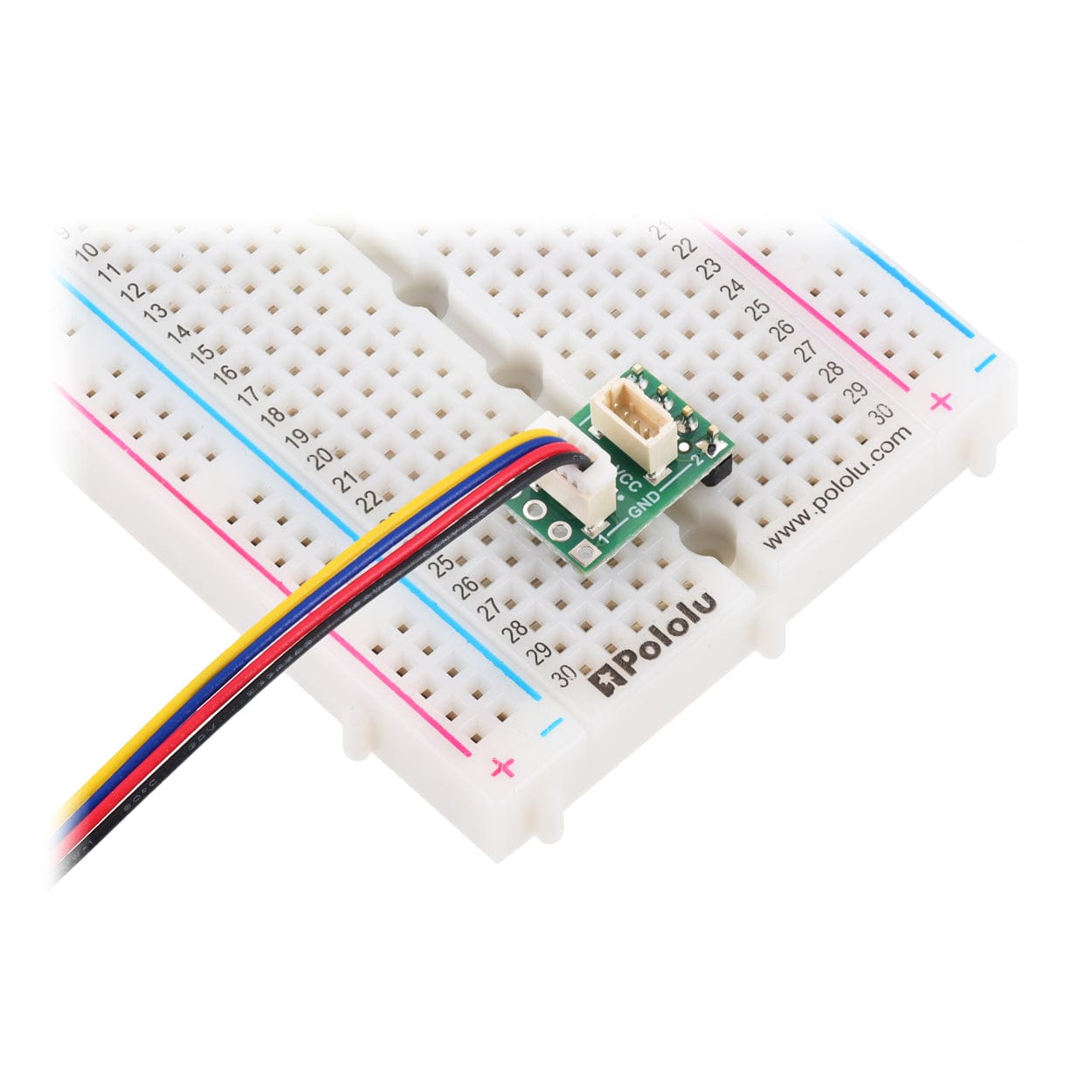
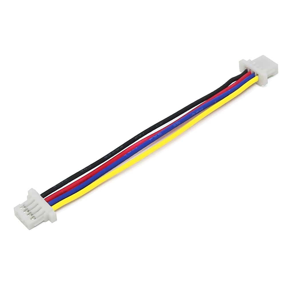
This is the version with JST-SH (Qwiic/STEMMA QT compatible) connectors, allowing easy connections with JST-SH 4-pin cables. We also stock a version with no connectors, which may be better for compact projects with directly soldered wires.

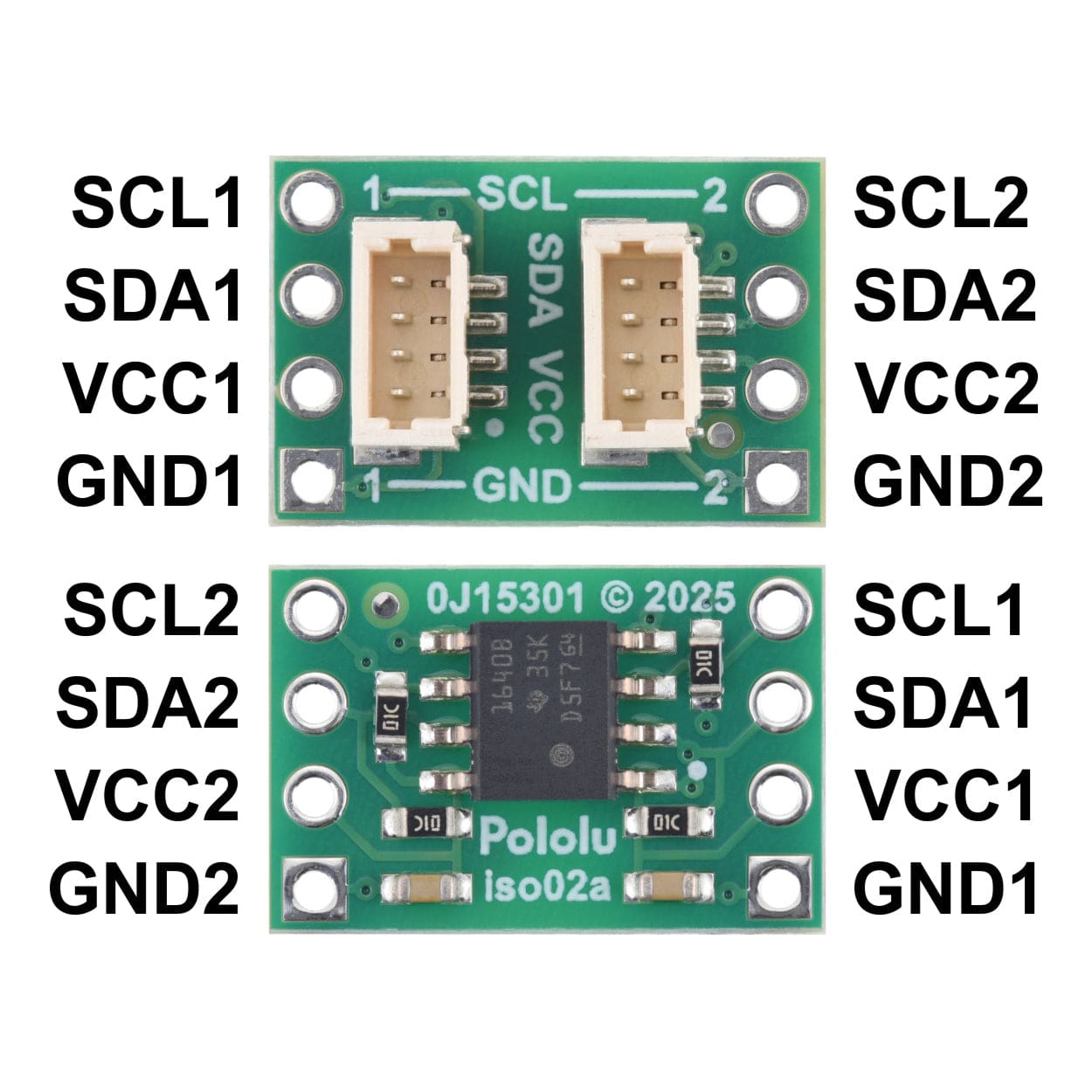
Each side must be powered separately: 3 V to 5.5 V should be supplied across VCC1 and GND1, and 2.25 V to 5.5 V should be supplied across VCC2 and GND2. The two sides are galvanically isolated (GND1 is NOT connected to GND2).
SDA1 and SCL1 connect to the I²C data and clock signals of one device, while SDA2 and SCL2 connect to the I²C data and clock signals of the other. Both the SDA and SCL connections are bidirectional, which allows for clock stretching. There are 10k pull-up resistors from SDA1 and SCL1 to VCC1 and from SDA2 and SCL2 to VCC2; for high-speed communication, external pull-up resistors can be added in parallel as necessary to make the pull-ups stronger.
Note: The two sides of the ISO1640 have different logic thresholds. In particular, SDA1 and SCL1 will only drive as low as 0.5 V to 0.7 V when the corresponding SDA2 or SCL2 are driven low, so it is important to ensure that the device connected to side 1 will recognize 0.7 V as low. In the other direction, SDA2 and SCL2 will drive to between 0 V and 0.4 V when SDA1 and SCL1 are driven low. See the ISO1640 datasheet for more information.
Although the ISO1640 IC has an isolation rating of up to 3 kVRMS, please note that the board is made to be compact, and the tightest clearance (2 mm) is smaller than the 4 mm clearance of the IC package. The picture below shows the regions of tightest clearance (the larger pads are just structural pads for the connectors and are not electrically connected to anything):
![]()
| Minimum operating voltage | 2.25 V |
| Minimum operating voltage | 3 V |
| Maximum operating voltage | 5.5 V |
| Connectors? | Y |
| Isolated power transfer? | N |
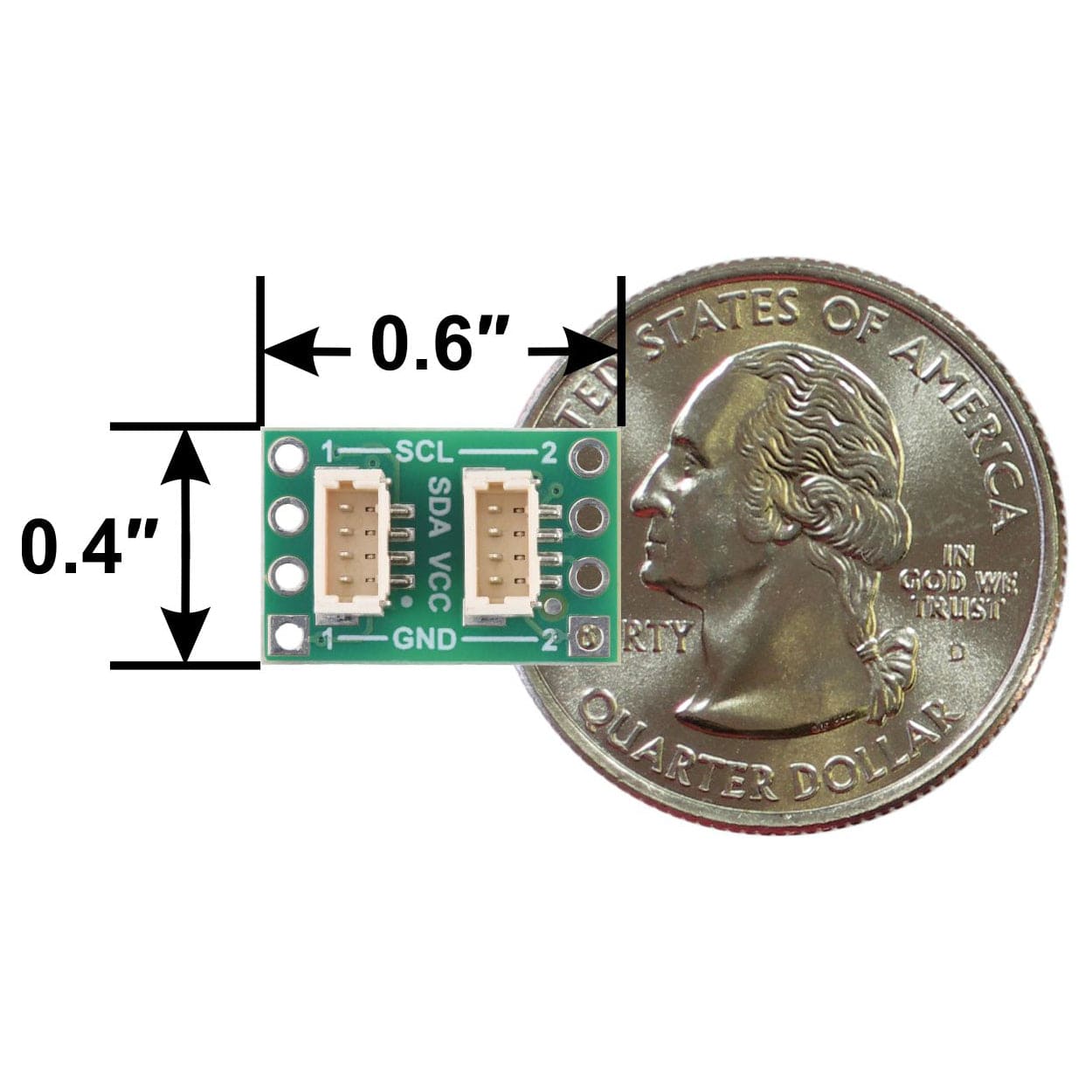
| Size | 0.4″ × 0.6″ × 0.28″ |
| Weight | 0.6 g |
Your payment information is processed securely. We do not store credit card details nor have access to your credit card information.