

Login / Signup
Cart
Your cart is empty
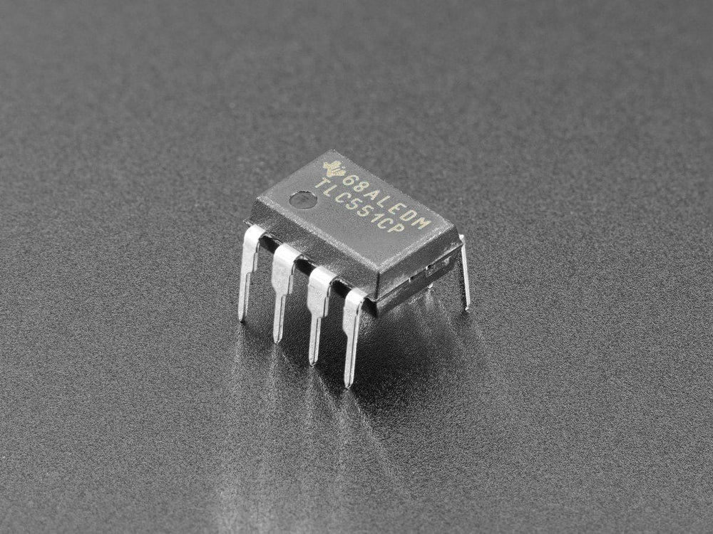
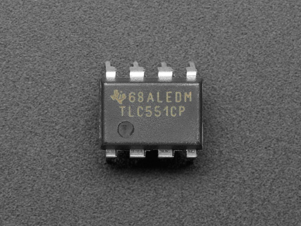
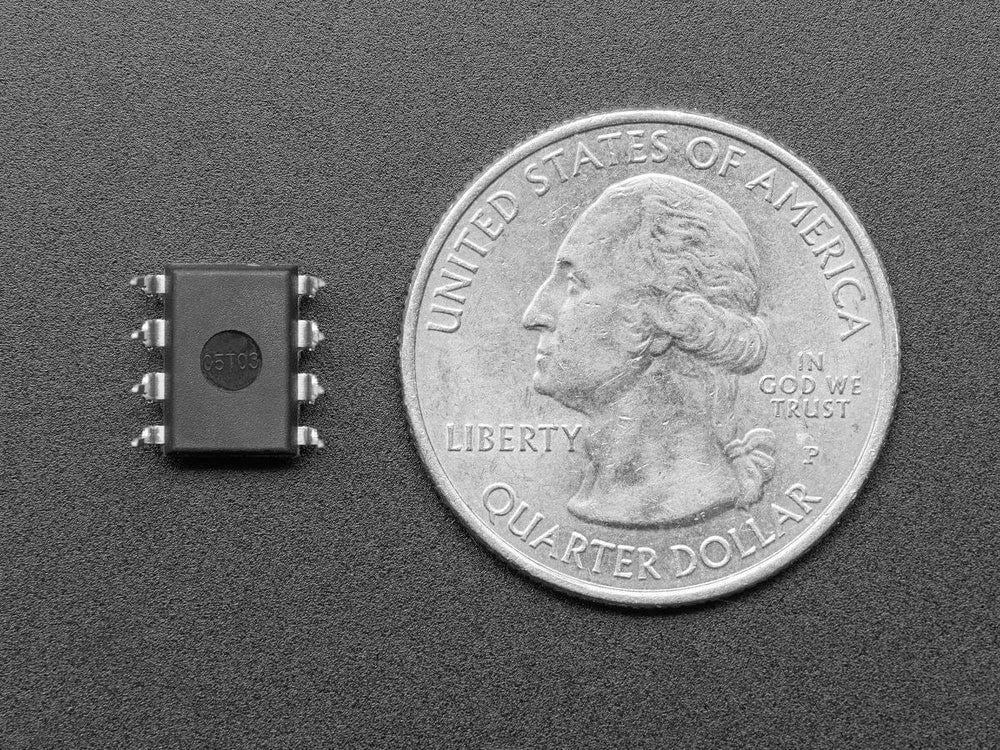
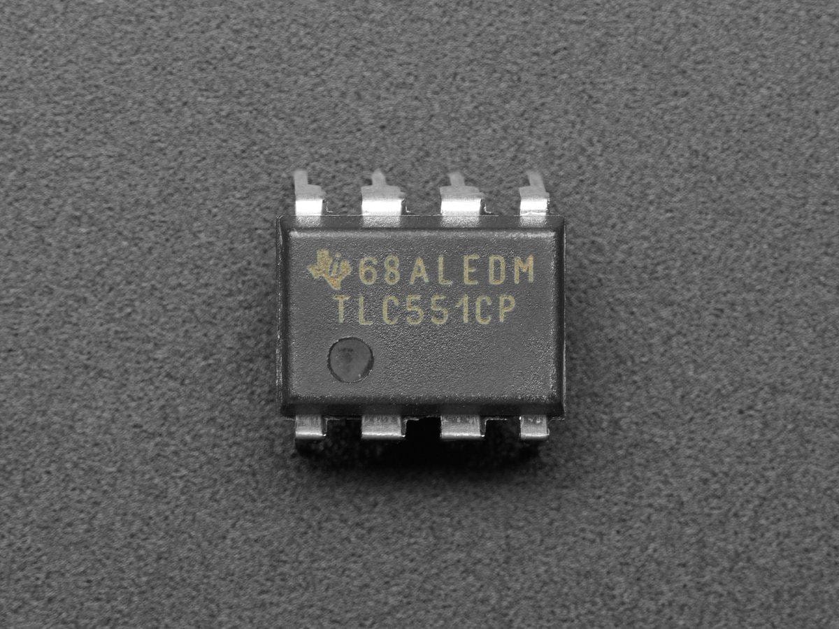
According to The Internet, 95% of electronic projects can be done with an op-amp or 555 timer chip. We're not so sure about it, but the 'triple nickel' (as we like to call it after we've had a gin&tonic) does come in handy for many simple analog or digital circuits. The classic part number is often referred to as the "NE555", and here we've got a modern spin on the classic.
The TLC551 is a monolithic timing circuit fabricated using TI's CMOS process, for lower power, wider voltage range, and higher speeds compared to 'classic' NE555s made with TTL. The timer is fully pin-compatible with CMOS, TTL, and MOS logic and operates at frequencies up to 2 MHz. Compared to the NE555 timer, this device uses smaller timing capacitors because of its high input impedance. As a result, more accurate time delays and oscillations are possible.
Power consumption is low across the full range of power supply voltage, so you can run it on even a single AAA, instead of needing a proper 5V or 9V power supply.
Like the NE555, the TLC551 has a trigger level equal to approximately one-third of the supply voltage and a threshold level equal to approximately two-thirds of the supply voltage. These levels can be altered by use of the control voltage terminal (CONT). When the trigger input (TRIG) falls below the trigger level, the flip-flop is set and the output goes high. If TRIG is above the trigger level and the threshold input (THRES) is above the threshold level, the flip-flop is reset and the output is low.
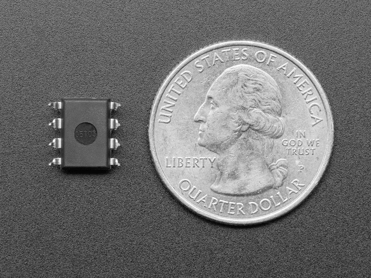
Comes as a single DIP chip for breadboard-friendly operation.
The reset input (RESET) can override all other inputs and can be used to initiate a new timing cycle. If RESET is low, the flip-flop is reset and the output is low. Whenever the output is low, a low-impedance path is provided between DISCH and GND. All unused inputs should be tied to an appropriate logic level to prevent false triggering.
While the CMOS output is capable of sinking over 100 mA and sourcing over 10 mA, the TLC551 exhibits greatly reduced supply-current spikes during output transitions. This minimizes the need for the large decoupling capacitors required by the NE555. The TLC551C is characterized for operation from 0°C to 70°C.

