Pololu Power ORing Ideal Diode Pair - 4-60V 6A
Price:
Sale price
£7.70
Stock:
Quantity:
Login / Signup
Cart
Your cart is empty
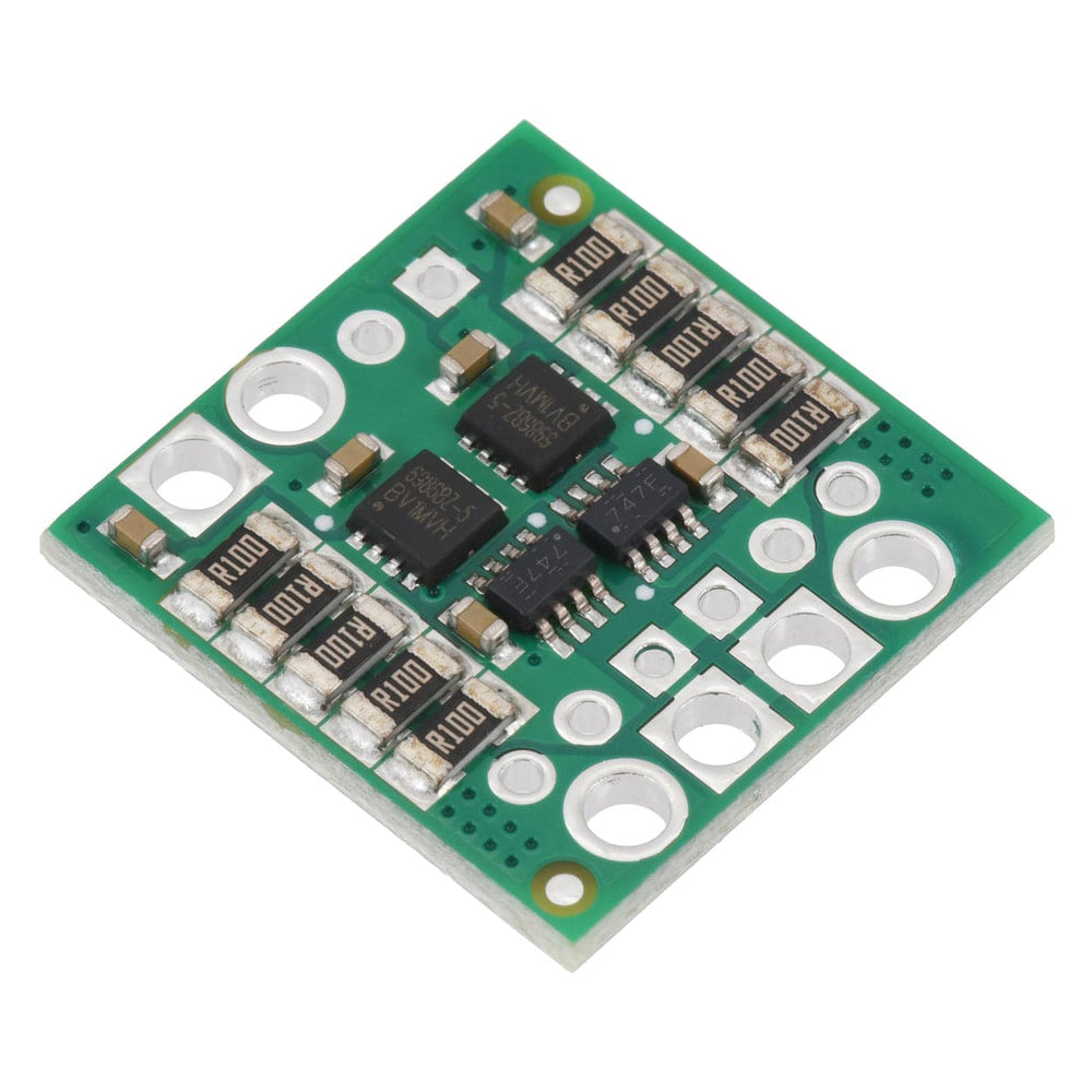
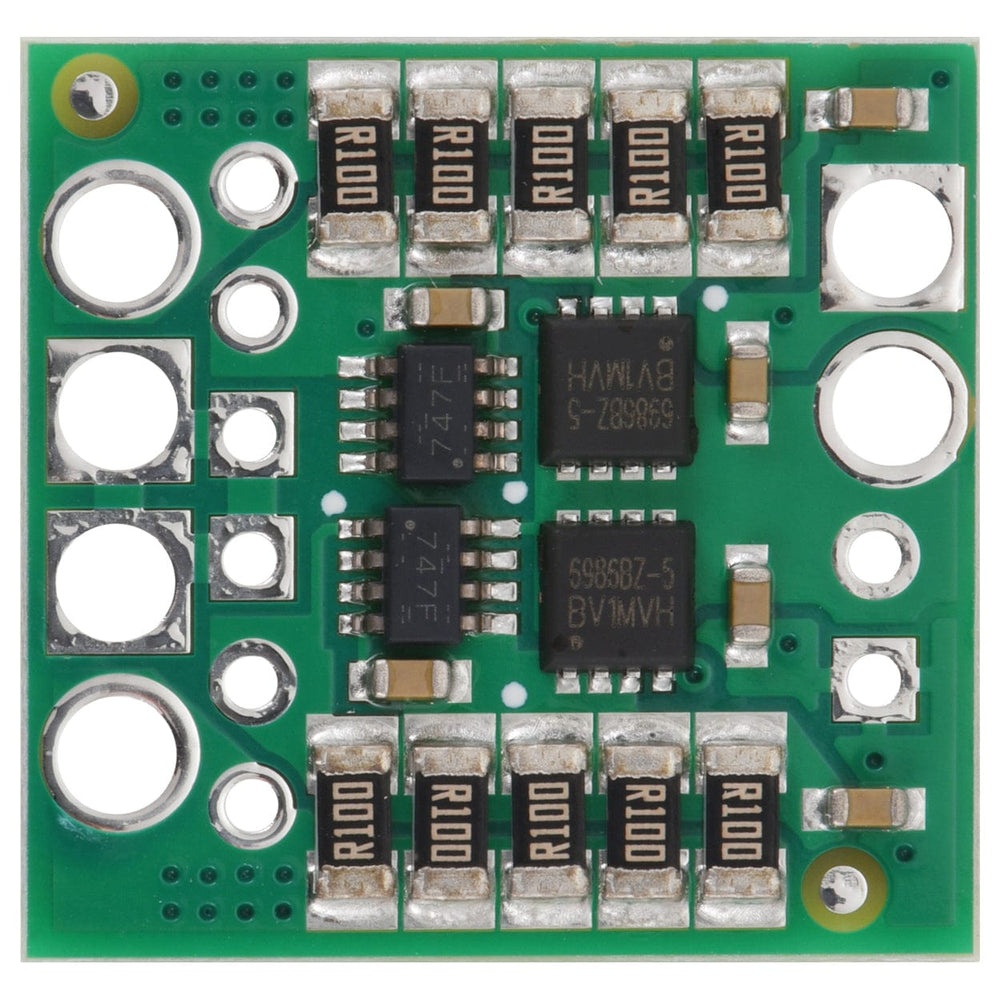


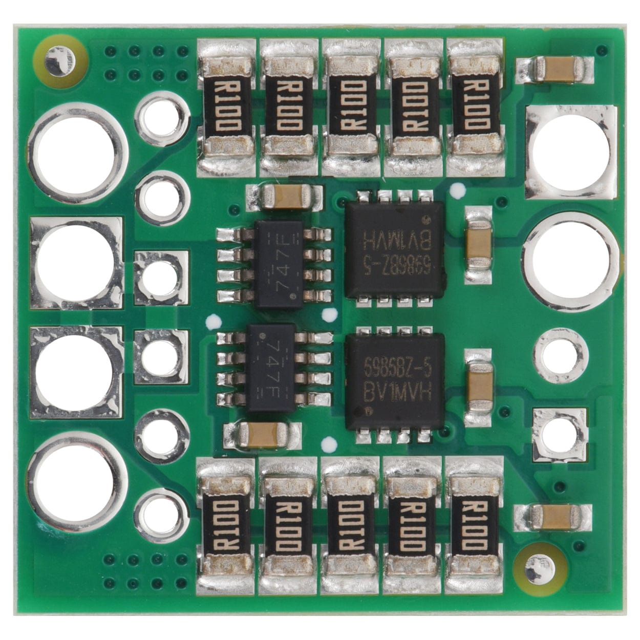
This module consists of two ideal diode circuits with their outputs connected to form a power ORing arrangement, which can be used for load sharing or for redundant (backup) power supplies. Each input has an inline, bypassable 20 mΩ resistance that can be used as a crude power balancing circuit.
This module consists of two identical ideal diode circuits with their outputs connected to form a power ORing arrangement. The ideal diodes prevent current from flowing from the output back into either input. Typical applications include redundant power supplies and power sharing.
Please note that since the two input sources are simply ORed together, there is no advanced selection option (e.g., there is no way to designate one input primary and the other secondary, and for all power to only come from that primary until it falls below a certain threshold before switching completely to the secondary supply).
The module can be used to split a large load across two smaller supplies, but the two supplies must have the same voltage for the load to be split evenly. A small 0.02 ohm resistance is available in line with each input to serve as a crude load-balancing mechanism. If you have two supplies with close voltages, you can either route both supplies through the extra resistance or only route the higher-voltage supply through the extra resistance. This approach can be extended to additional external resistance in line with the higher-voltage supply, or physically arranging and wiring modules such that the higher-voltage supply is farther from the power ORing circuit, adding more wire resistance to the path of the higher-voltage supply.

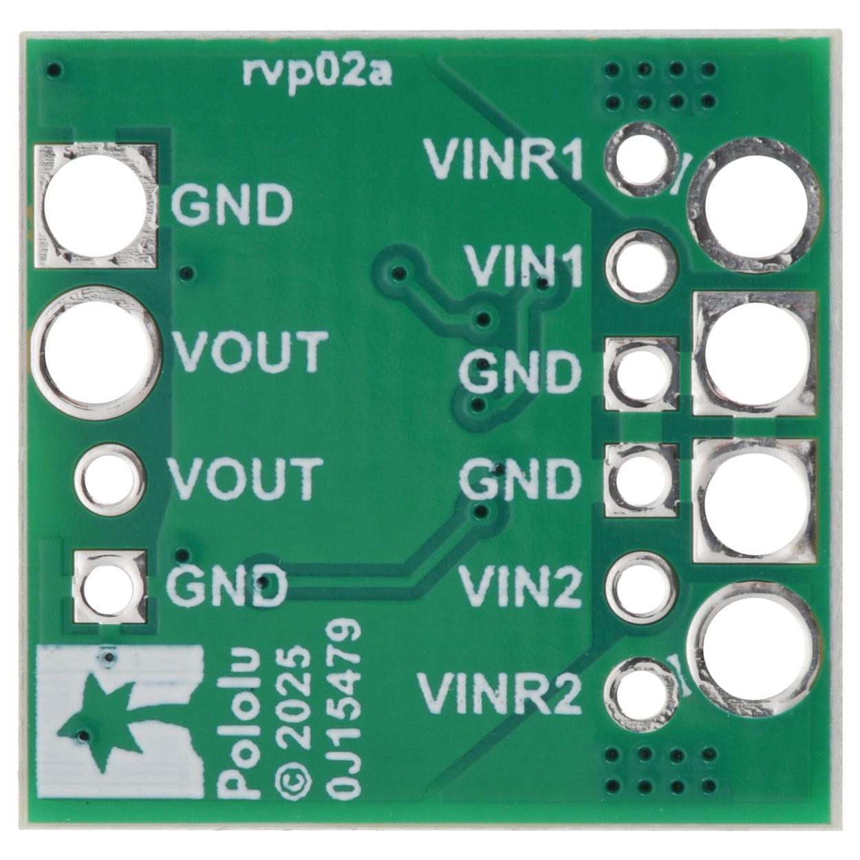
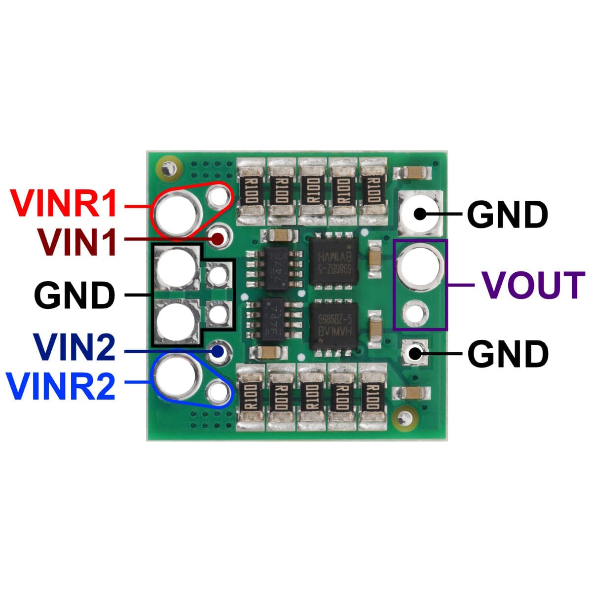
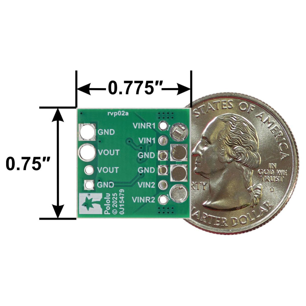
The input side of the board provides the connection points for the two input power supplies. For each supply, there are two connection options: VINRx, which goes through an equivalent 20 mΩ balancing resistor, and VINx, which bypasses the balancing resistor. The output side of the board provides the single ORed output, VOUT. The grounds are common everywhere on the board.
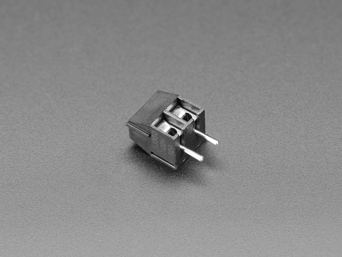
Connections can be made to the board through large 3.5mm-pitch through-holes, which are sized for 14 AWG wires and compatible with 3.5mm-pitch terminal blocks, or smaller 0.1″-pitch through-holes. On the input side, the large through-holes go through the balancing resistors (VINRx) while the small through-holes provide access to both VINRx and VINx. These smaller holes can be used directly as inputs, or they can be used as bypass jumpers for the larger inputs (i.e. by shorting the small VINRx and VINx pads).
The maximum allowable current is limited by thermal considerations, primarily in the load-balancing resistors that can allow up to 6 A at 25°C ambient temperature with no forced air flow. Please note that the board and its components will get very hot even at substantially lower currents. If the resistors are bypassed, the MOSFETs become the limiting component, and those can conduct 7 A or more under similar conditions. With sufficient cooling, up to 10 A per side is possible.
Warning: Exceeding temperature or current limits can cause permanent damage to the board components. If your average continuous current is greater than around 4 A per channel, we strongly recommend that you monitor the MOSFETs’ temperature and look into additional cooling if necessary.
Warning: This product can get hot enough to burn you long before the components overheat. Take care when handling this product and other components connected to it.
| Size | 0.75″ × 0.775″ × 0.11″ |
| Weight | 1.4 g |
| Minimum operating voltage | 4 V1 |
| Maximum operating voltage | 60 V |
| Maximum current | 6 A2 |
| Reverse current blocking | Y |
| PCB dev codes | rvp02a |
| Other PCB markings | 0J15479 |
Your payment information is processed securely. We do not store credit card details nor have access to your credit card information.