

Login / Signup
Cart
Your cart is empty
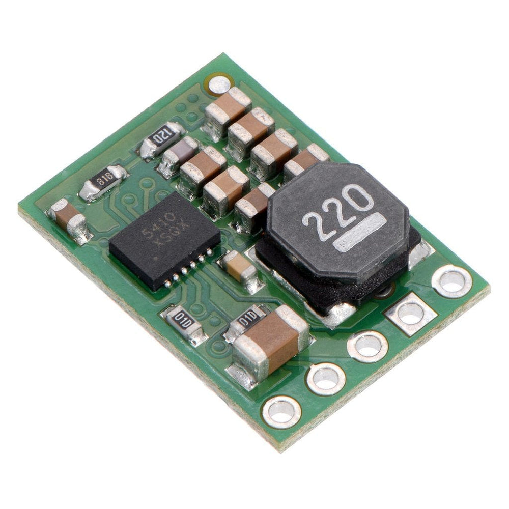
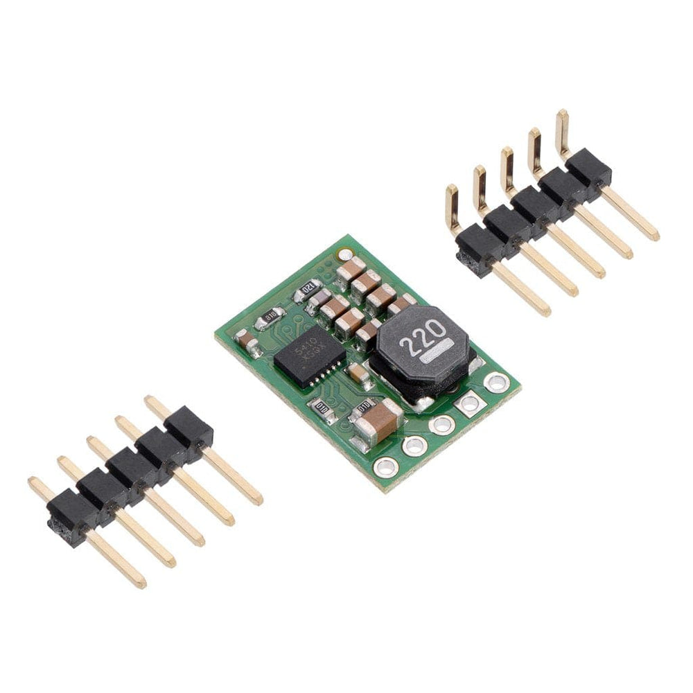


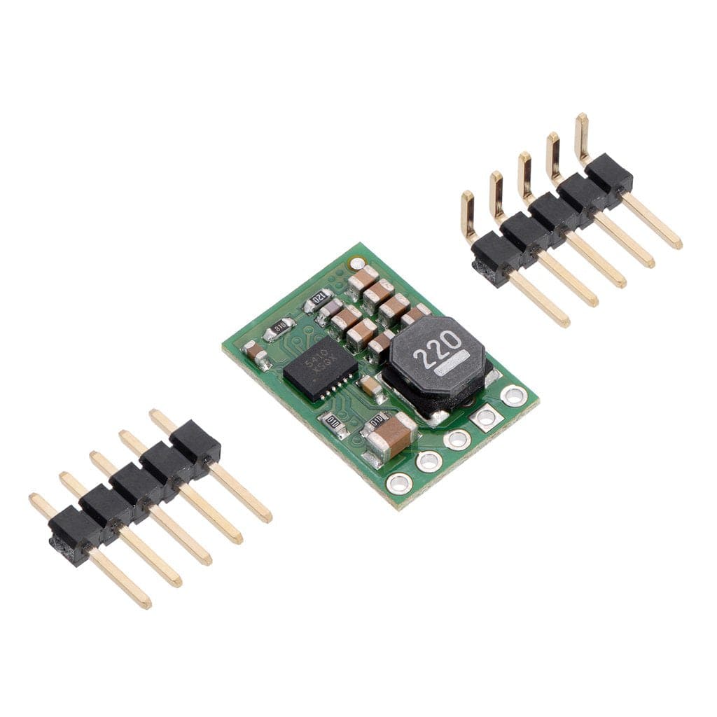
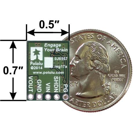
The compact (0.5″ × 0.7″) D24V10F9 synchronous buck voltage regulator takes an input voltage of up to 36 V and efficiently reduces it to 9 V while allowing for a maximum output current of 1 A.
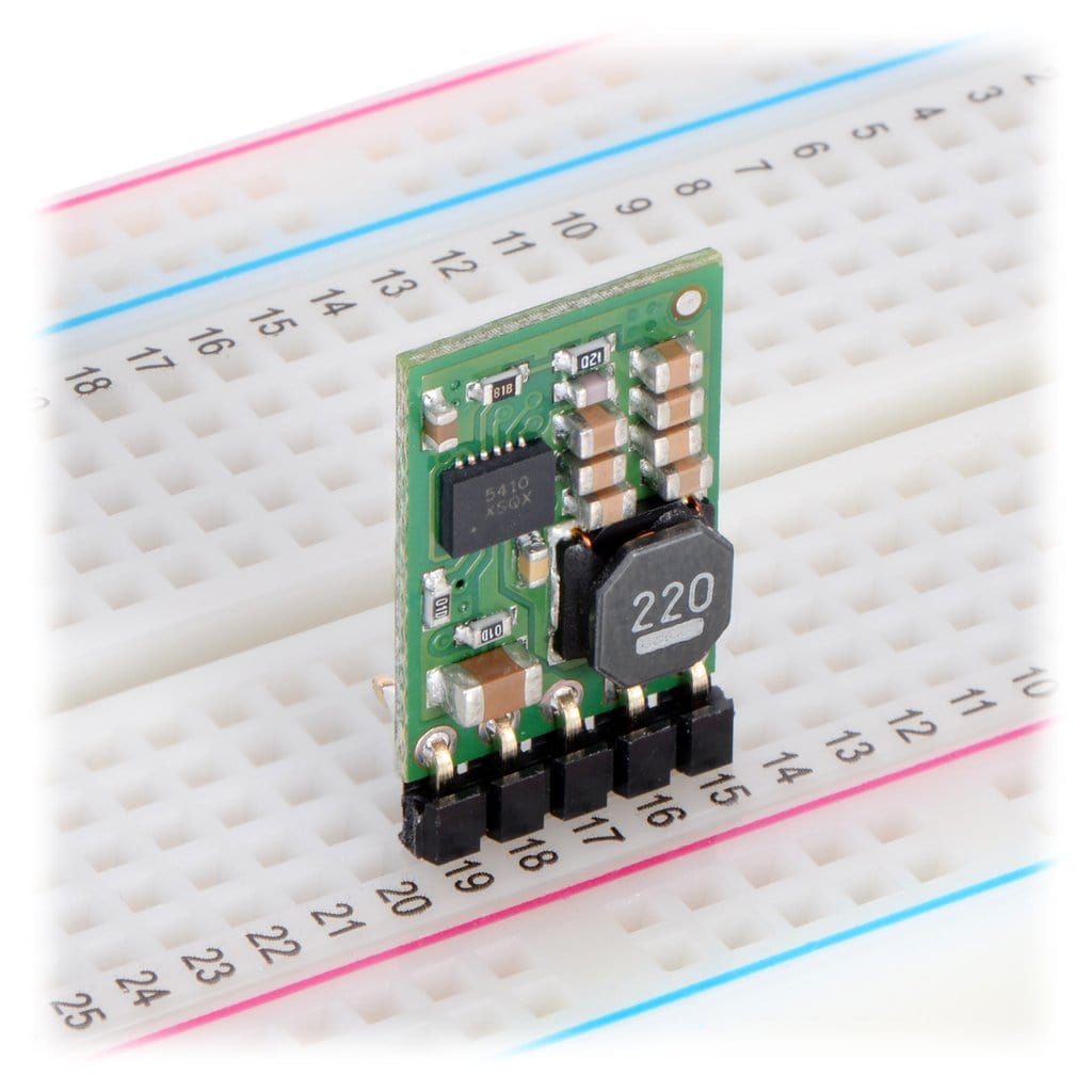
This regulator offers typical efficiencies between 85% and 93% and has a very low dropout, so it can be used with input voltages as low as a few hundred millivolts above 9 V. The pins have a 0.1″ spacing, making this board compatible with standard solderless breadboards and perfboards.
The D24V10Fx family of step-down voltage regulators features the Intersil ISL85410 1A synchronous buck regulator and generates lower output voltages from input voltages as high as 36 V. They are switching regulators (also called switched-mode power supplies (SMPS) or DC-to-DC converters) with typical efficiencies between 80% and 95%, which is much more efficient than linear voltage regulators, especially when the difference between the input and output voltage is large. These regulators have a power-save mode that activates at light loads and a low quiescent (no load) current draw, which make them well suited for applications that are run from a battery.
The SHDN pin can be used to put the board in a low-power state that reduces the quiescent current to approximately 10 µA to 20 µA per volt on VIN, and a PG (power good) output can be used to monitor the state of the regulator’s output voltage.
The regulators feature short-circuit/over-current protection, and thermal shutdown helps prevent damage from overheating. The boards do not have reverse-voltage protection.
1Without included optional headers.
2For small loads; this voltage rises approximately linearly up to 9.8 V at 1 A output.
3While enabled (SHDN = HIGH) with no load; while disabled it is proportional to the input voltage (360 μA when the input is 36 V).
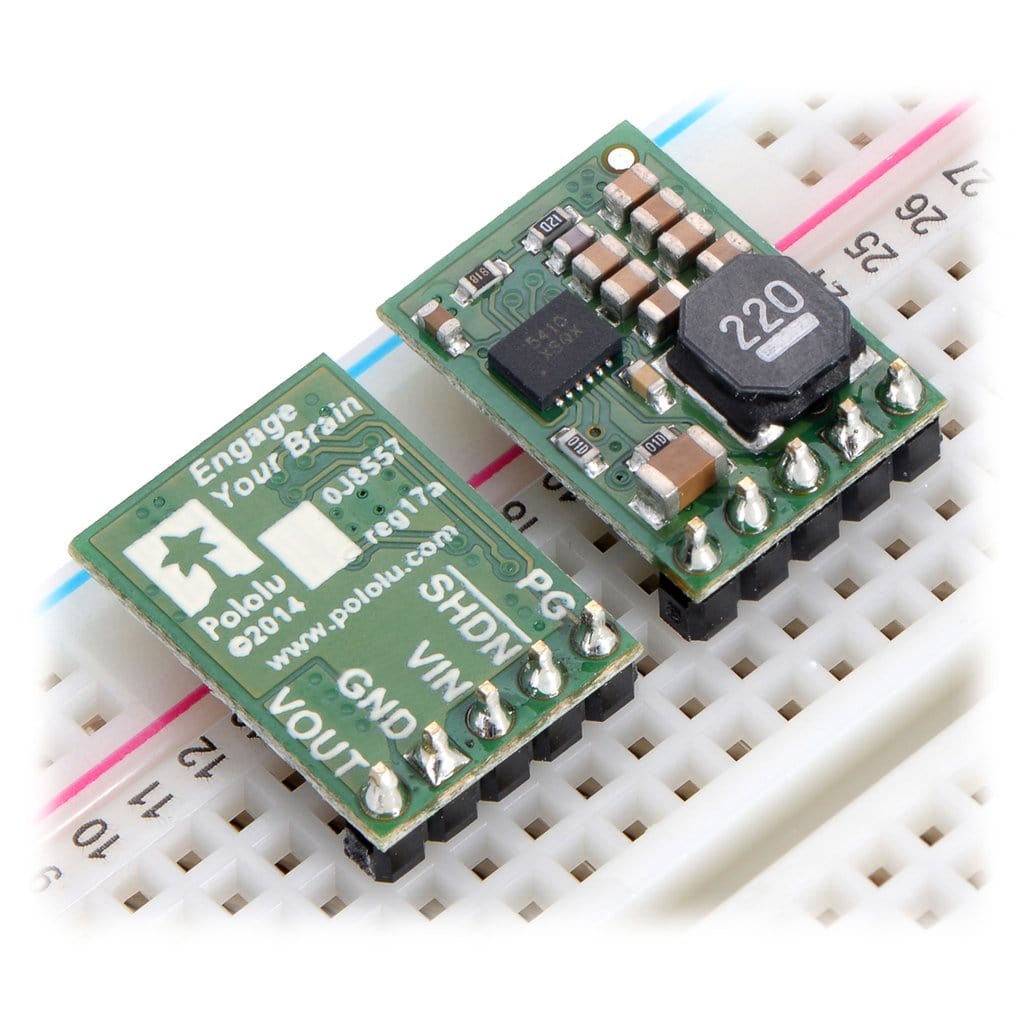
The buck regulator has five connections: power good (PG). shutdown (SHDN), input voltage (VIN), ground (GND), and output voltage (VOUT).
The “power good” indicator, PG, is an open-drain output that drives low when the regulator’s output voltage falls below 80% or rises above 120% of its target output voltage. This output is also actively held low for the duration of the regulator’s 2 ms soft-start period and while the regulator is being disabled by the SHDN input or by over-temperature or over-current fault conditions. An external pull-up resistor is generally required to use this pin.
The SHDN pin can be driven low (under 0.4 V) to turn off the output and put the board into a low-power state. There is a 100 kΩ pull-up resistor between the SHDN pin and VIN, so if you want to leave the board permanently enabled, the SHDN pin can be left disconnected. While the SHDN pin is being driven low, the current draw of the regulator is dominated by the current through the pull-up resistor and will be proportional to the input voltage. (At 36 V in it will draw about 360 μA.)
The input voltage, VIN, powers the regulator. Voltages between 3 V and 36 V can be applied to VIN, but the effective lower limit of VIN is VOUT plus the regulator’s dropout voltage, which varies approximately linearly with the load (see below for graphs of dropout voltages as a function of the load). Additionally, please be wary of destructive LC spikes (see below for more information).
The output voltage, VOUT, is fixed and depends on the regulator version: the D24V10F3 version outputs 3.3 V, the D24V10F5 version outputs 5 V, the D24V10F6 version outputs 6 V, the D24V10F9 version outputs 9 V, and the D24V10F12 version outputs 12 V.
The efficiency of a voltage regulator, defined as (Power out)/(Power in), is an important measure of its performance, especially when battery life or heat are concerns. This family of switching regulators typically has an efficiency of 80% to 93%, though the actual efficiency in a given system depends on input voltage, output voltage, and output current. See the efficiency graph near the bottom of this page for more information.
In order to achieve a high efficiency at low loads, this regulator automatically goes into a power-save mode where the switching frequency is reduced. In power-save mode, the switching frequency of the regulator changes as necessary to minimize power loss. This could make it harder to filter out noise on the output caused by switching.
The dropout voltage of a step-down regulator is the minimum amount by which the input voltage must exceed the regulator’s target output voltage in order to ensure the target output can be achieved. For example, if a 5 V regulator has a 1 V dropout voltage, the input must be at least 6 V to ensure the output is the full 5 V. Generally speaking, the dropout voltage increases as the output current increases.
The graphs below show the typical efficiency and dropout voltage of the 9 V D24V10F9 regulator as a function of the output current:


When connecting voltage to electronic circuits, the initial rush of current can cause voltage spikes that are much higher than the input voltage. If these spikes exceed the regulator’s maximum voltage (36 V), the regulator can be destroyed. In our tests with typical power leads (~30″ test clips), input voltages above 20 V caused spikes over 36 V.
If you are connecting more than 20 V or your power leads or supply has high inductance, we recommend soldering a 33 μF or larger electrolytic capacitor close to the regulator between VIN and GND. The capacitor should be rated for at least 50 V.
More information about LC spikes can be found in this application note, Understanding Destructive LC Voltage Spikes.

