Pololu 5V Step-Up Voltage Regulator U1V11F5
Price:
Sale price
£7.70
Stock:
Quantity:
Login / Signup
Cart
Your cart is empty
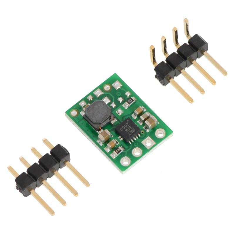
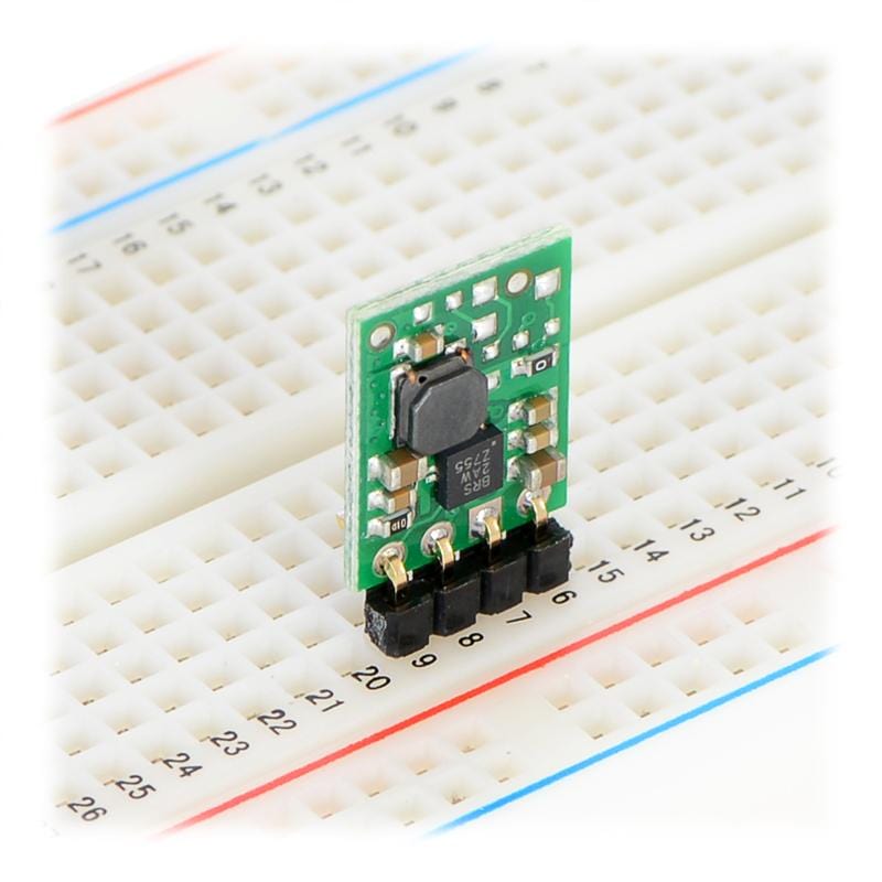

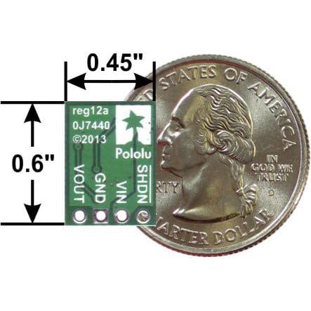
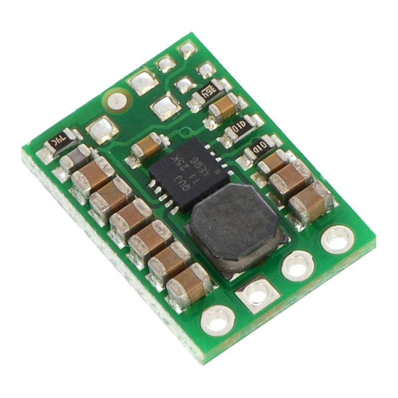
This compact (0.45″×0.6″) U1V11F5 switching step-up (or boost) voltage regulator efficiently generates 5 V from input voltages as low as 0.5 V.
Unlike most boost regulators, the U1V11F5 offers a true shutdown option that turns off power to the load, and it automatically switches to a linear down-regulation mode when the input voltage exceeds the output. The pins have a 0.1″ spacing, making this board compatible with standard solderless breadboards and perfboards.
This 5 V boost (step-up) voltage regulator generates higher output voltages from input voltages as low as 0.5 V, and it also automatically switches to a linear down-regulation mode when the input voltage exceeds the output. This makes it great for powering 5 V electronics projects from 1 to 3 NiMH, NiCd, or alkaline cells or from a single lithium-ion cell. Additionally, unlike most boost regulators, this unit offers a true shutdown option that turns off power to the load (with typical boost regulators, the input voltage will pass directly through to the output when they are disabled).
When boosting, this module acts as a switching regulator (also called switched-mode power supplies (SMPS) or DC-to-DC converters) and has a typical efficiency between 70% to 90%. The available output current is a function of the input voltage, output voltage, and efficiency (see Typical Efficiency and Output Current section below), but the input current can typically be as high as 1.2 A.
The regulator’s thermal shutdown engages at around 140°C and helps prevent damage from overheating, but it does not have reverse-voltage protection.
Connections
The boost regulator has four connections: shutdown (SHDN), input voltage (VIN), ground (GND), and output voltage (VOUT).
The SHDN can be driven low (typically under 0.4 V) to power down the regulator and turn off power to the load (unlike most boost regulators, the input power does not pass through to the output when the board is disabled). This pin is internally pulled up to VIN through an 100 kΩ resistor, so it can be left disconnected or connected directly to VIN if you do not need to use the disable feature. The disable threshold is a function of the input voltage as follows:
The input voltage, VIN, must be at least 0.5 V for the regulator to turn on. However, once the regulator is on, the input voltage can drop as low as 0.3 V and the 5 V output voltage will be maintained on VOUT. Unlike standard boost regulators, this regulator has an additional linear down-regulation mode that allows it to convert input voltages as high as 5.5 V down to 5 V for small to moderate sized loads. When the input voltage exceeds 5 V, the regulator automatically switches to this down-regulation mode. The input voltage should not exceed 5.5 V. Please be wary of destructive LC spikes that might cause the input voltage to surpass 5.5 V (see below for more information).
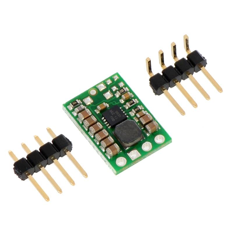
The four connections are labeled on the back side of the PCB, and they are arranged with a 0.1″ spacing along the edge of the board for compatibility with solderless breadboards, connectors, and other prototyping arrangements that use a 0.1″ grid. You can solder wires directly to the board or solder in either the 4×1 straight male header strip or the 4×1 right-angle male header strip that is included.
The efficiency of a voltage regulator, defined as (Power out)/(Power in), is an important measure of its performance, especially when battery life or heat are concerns. As shown in the graphs below, this switching regulator typically has an efficiency of 70 to 90%.
The maximum achievable output current is approximately proportional to the ratio of the input voltage to the output voltage. If the input current exceeds the switch current limit (typically somewhere between 1.2 and 1.5 A), the output voltage will begin to drop. Additionally, the maximum output current can depend on other factors, including the ambient temperature, air flow, and heat sinking.
When connecting voltage to electronic circuits, the initial rush of current can cause damaging voltage spikes that are much higher than the input voltage. In our tests with typical power leads (~30″ test clips), input voltages above 4.5 V caused voltage spikes that could potentially damage the regulator. You can suppress such spikes by soldering a 33 μF or larger electrolytic capacitor close to the regulator between VIN and GND.
More information about LC spikes can be found in this application note, Understanding Destructive LC Voltage Spikes.
Your payment information is processed securely. We do not store credit card details nor have access to your credit card information.