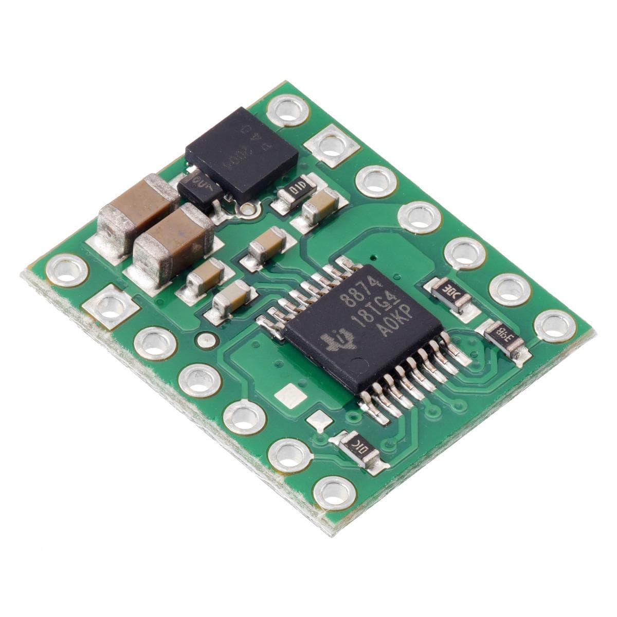
Pololu DRV8874 Single Brushed DC Motor Driver Carrier
Price:
Sale price
£11.50
Stock:
Cart
Your cart is empty


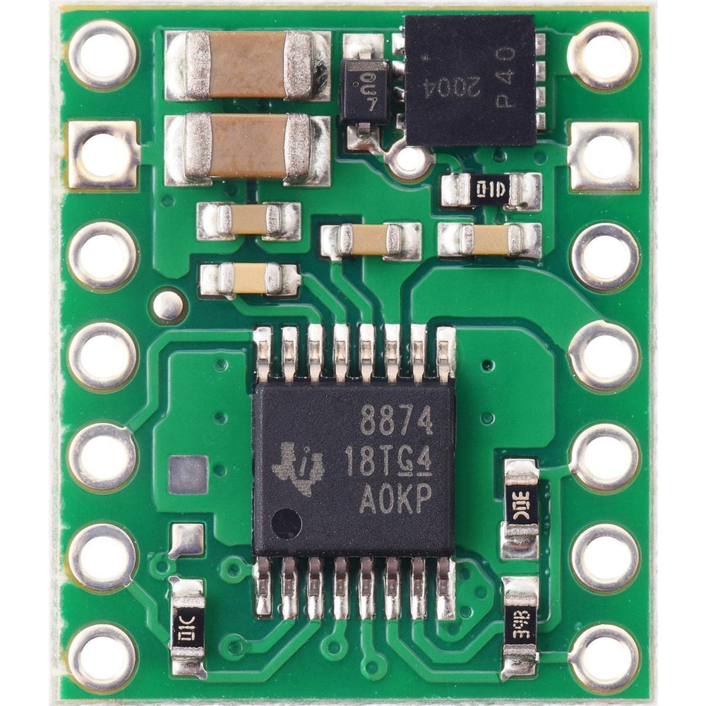
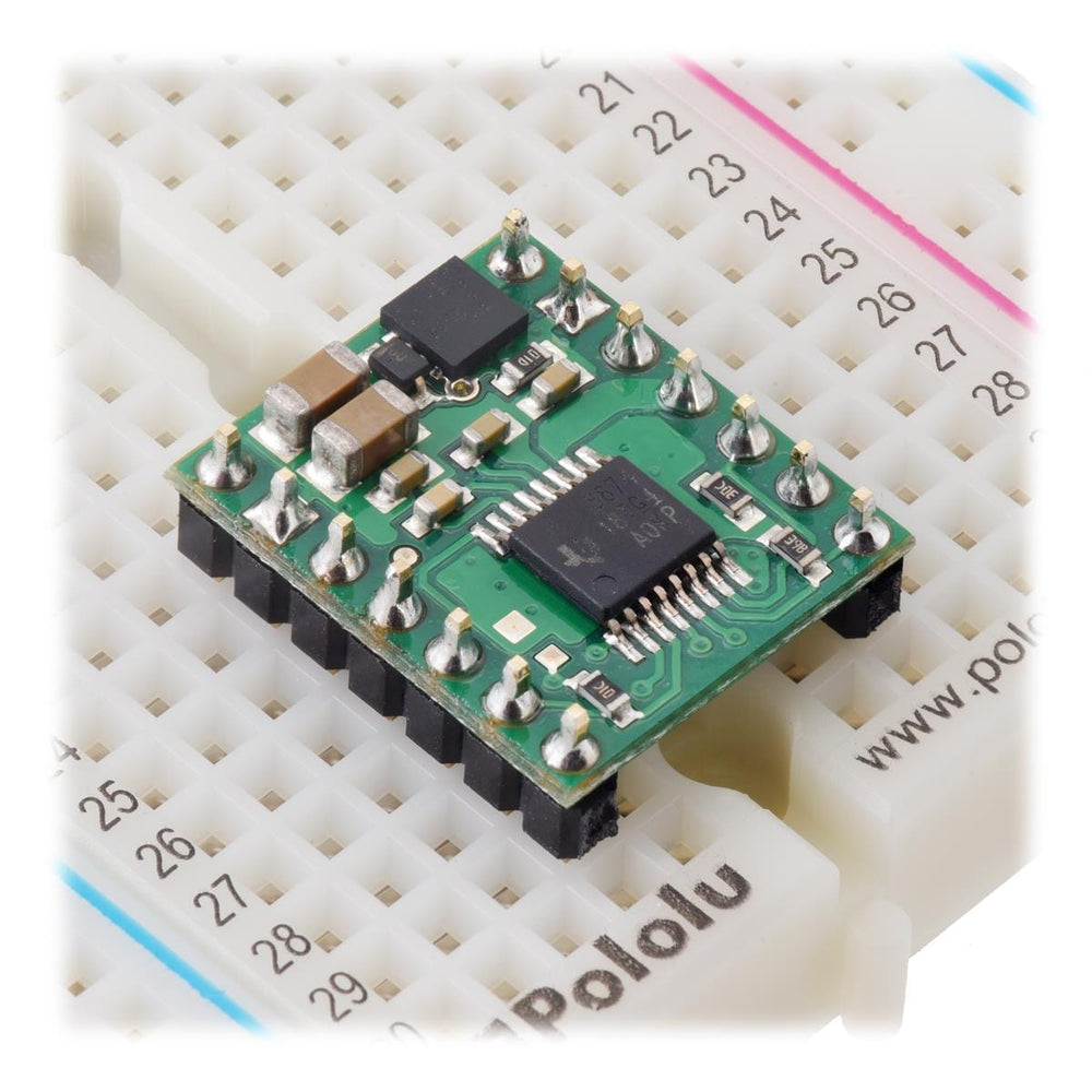
This compact Pololu breakout board for TI’s DRV8874 motor driver offers a wide operating voltage range of 4.5V to 37V and can deliver a continuous 2.1A (6A peak) to a single bidirectional brushed DC motor. The DRV8874 also features integrated current sensing and regulation as well as built-in protection against under-voltage, over-current, and over-temperature. The carrier board adds protection against reverse voltage.
Since this board is a carrier for the DRV8874, we recommend careful reading of the DRV8874 datasheet. The board ships populated with all of its SMD components, including the DRV8874.
Warning: This product can get hot enough to burn you long before the chip overheats. Take care when handling this product and other components connected to it.
| Motor driver | DRV8874 |
| Motor channels | 1 |
| Minimum operating voltage | 4.5 V |
| Maximum operating voltage | 37 V |
| Continuous output current per channel | 2.1 A |
| Peak output current per channel | 6A |
| Current sense | 1.13 V/A |
| Maximum PWM frequency | 100 kHz |
| Minimum logic voltage | 1.8 V |
| Maximum logic voltage | 5.5 V |
| Reverse voltage protection? | Y |
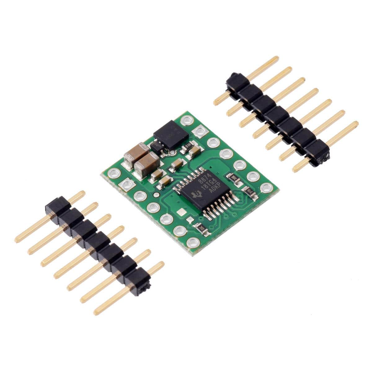
| Header pins soldered? | N |
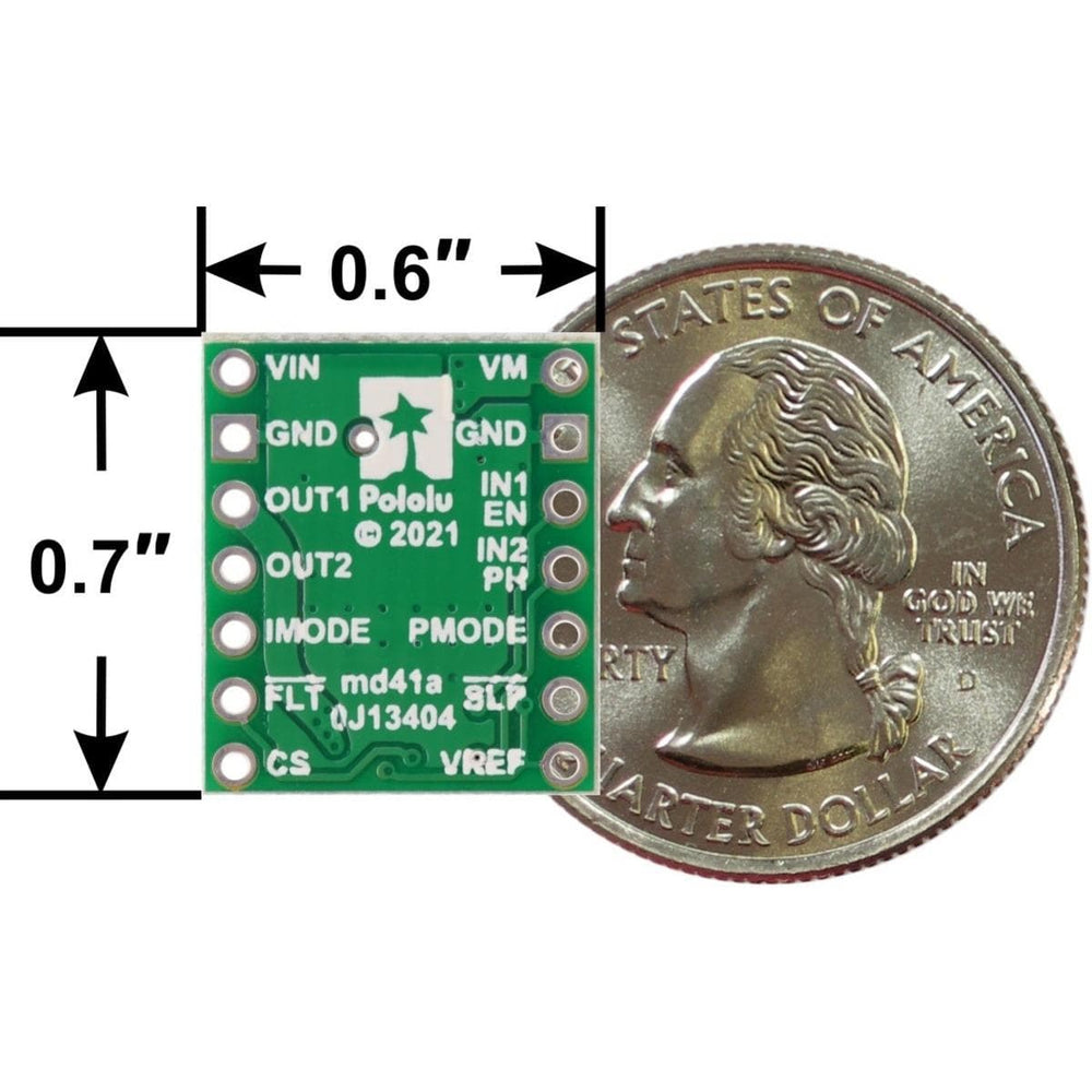
| Size | 0.6″ × 0.7″ |
| Weight | 0.9 g |
Breakaway 0.1″ male headers are included with the motor driver carrier, which can be soldered in to use the driver with perfboards, breadboards, or 0.1″ female connectors (the headers might ship as a single larger strip that can be broken into smaller pieces).
When used with these header pins, the board can be oriented with the parts visible or with the silkscreen visible, by soldering the headers in from the opposite side. You can also solder your motor leads and other connections directly to the board.

Motor and motor power connections are made on one side of the board and logic power and control connections are made on the other. The driver requires a motor voltage between 4.5 V and 37 V to be supplied to the VIN or VM pin. The driver is in sleep mode by default, and a logic voltage between 1.8 V and 5.5 V must be supplied to the SLEEP pin; to take it out of sleep mode. This logic voltage can typically shared with the controlling device, or it can be supplied by an output from the controlling device, which allows for dynamic control of the sleep mode. The VIN pin is the reverse-protected motor supply input and is the recommended point for connecting motor power. VM is an access point for motor supply power after the reverse voltage protection circuit.
The DRV8874 features three possible control modes: phase/enable (PH/EN), PWM (IN/IN), and independent half-bridge. The PMODE pin determines the control interface, and the state is latched when the driver is enabled through the SLEEP pin.
Setting the PMODE pin low prior to enabling the driver, as shown in the diagram above, sets the driver to phase/enable control mode, where the PH pin determines the motor direction and the EN pin can be supplied with a PWM signal to control the motor speed (this is typically referred to as sign-magnitude operation). This mode is generally easier to use as it only requires one PWM signal, but it only allows for drive/brake operation. (Drive/brake operation usually provides a more linear relationship between PWM duty cycle and motor speed than drive/coast operation, and we generally recommend using drive/brake operation when possible.)
| Simplified drive/brake operation with PMODE=0 (PHASE/ENABLE) | ||||
| EN | PH | OUT1 | OUT2 | Operating mode |
| 0 | X | L | L | brake low (outputs shorted to ground) |
| PWM | 1 | PWM (H/L) | L | forward/brake at speed PWM % |
| PWM | 0 | L | PWM (H/L) | reverse/brake at speed PWM % |
This mode can also be used for locked-antiphase operation, where a sufficiently high-frequency (up to 100 kHz) PWM is applied to the phase (PH) pin and the enable (EN) pin is tied high. In locked-antiphase operation, the PWM duty cycle controls speed and direction, going from full-speed in one direction at 0% duty cycle to full speed in the other direction at 100% duty cycle. A duty cycle of 50% will stop the motor. The appropriate PWM frequency will generally depend on the inductance of the motor.

When the PMODE pin is set high prior to enabling the driver, the driver is set to PWM (IN/IN) control mode, which allows for more advanced control options, including allowing the H-bridge to enter a high-impedance (coast) state without having to put it to driver sleep. The following truth table show how to achieve drive/coast (slow decay) and drive/brake (fast decay) operation using the IN/IN control interface:
| PWM control mode with PMODE=1 (IN/IN) | ||||
| IN1 | IN2 | OUT1 | OUT2 | operating mode |
| 0 | 0 | Z | Z | coast (outputs off) |
| PWM | 0 | PWM (H/Z) | PWM (L/Z) | forward/coast at speed PWM % |
| 0 | PWM | PWM (L/Z) | PWM (H/Z) | reverse/coast at speed PWM % |
| PWM | 1 | L | PWM (L/H) | reverse/brake at speed 100% − PWM % |
| 1 | PWM | PWM (L/H) | L | forward/brake at speed 100% − PWM % |
| 1 | 1 | L | L | brake low (outputs shorted to ground) |
When the PMODE pin is left high-impedance (i.e. floating or disconnected) when the driver is enabled, the driver is set to independent half-bridge control mode. See the datasheet for more information about this control mode.

| PIN | Default State | Description |
| VIN | 4.5 V to 37 V board power supply input. | |
| GND | Ground connection points for the motor and logic supplies. The control source and the motor driver must share a common ground. | |
| VM | This pin gives access to the motor power supply after the reverse-voltage protection MOSFET (see the board schematic below). It can be used to supply reverse-protected power to other components in the system. | |
| OUT1 | Motor output 1. | |
| OUT2 | Motor output 2. | |
| EN/IN1 | LOW | Motor control input 1 (functions as an enable pin in PHASE/ENABLE mode). |
| PH/IN2 | LOW | Motor control input 2 (functions as a direction pin in PHASE/ENABLE mode). |
| PMODE | FLOATING | Control interface select pin. The state of this pin is latched when the driver is enabled through the SLEEP pin. Setting this pin low prior to enabling sets the driver to phase/enable (PH/EN) control mode. Setting this pin high prior to enabling sets the driver to PWM (IN/IN) control mode. Leaving this pin floating or disconnected on enable sets the driver to independent half-bridge control mode. |
| SLEEP | LOW | Sleep input that puts the driver into a low-power sleep mode when low. The driver outputs are high-impedance (coast) in sleep mode. |
| VREF | Current limiting threshold reference voltage (see below). | |
| IMODE | PULLED LOW | Four-state input for current regulation and overcurrent protection mode (see below). This carrier pulls down IMODE to GND through a 20 kΩ resistor setting the current chopping mode to cycle-by-cycle, the over-current response to automatic retry, and FAULT response to current chopping and over-current. |
| FAULT | FLOATING | Open-drain, active-low fault output. This pin goes low during an over-current, over-temperature, or under-voltage condition. An external pull-up resistor is required to use this pin. |
| CS | Current sense output. This pin provides an analog current-sense feedback voltage of approximately 1.1 V/A (DRV8874) or 2.5 V/A (DRV8876). |
The DRV8874/DRV8876 can be configured to actively limit the current through the motors by using a fixed off-time PWM current regulation (current chopping) or a cycle-by-cycle PWM current chopping scheme.
The current chopping scheme and over-current response is selectable through the IMODE quad-level input. This carrier pulls down IMODE to GND through a 20 kΩ resistor, setting the current chopping mode to cycle-by-cycle. The current limit is determined by the voltage on the VREF pin, which this carrier board pulls up to SLEEP through a 10 kΩ resistor, and the resistor on the CS pin, which this carrier board pulls down to GND through a 2.49 kΩ resistor.
When SLEEP is connected to 5 V, the current limit is set to approximately 4.4 A on the DRV8874 carrier. The current limit can be lowered by connecting an additional resistor between VREF and GND or by connecting an external reference voltage directly to VREF; the current limit can be increased by connecting an additional resistor between CS and GND. Current limiting can be disabled by connecting CS directly to GND. Refer to the datasheet for more information about the driver’s current regulation.
The DRV8874 is rated for a peak current of 6 A. However, the chips by themselves will overheat at lower currents. In our tests, we found that the chips on our carrier boards were able to deliver their rated peak currents for less than a second before their thermal protection kicked in and disabled the motor outputs. They were able to operate at their default current limits of 4.4 A for a few seconds before thermal shutdown. The continuous current specifications we provide for these boards of 2.1A we found to be sustainable for many minutes without triggering thermal shutdown. These tests were conducted at room temperature in an open space with no additional cooling (e.g. no forced airflow or heat sinks).
The actual current you can deliver will depend on how well you can keep the motor driver cool. The carrier’s printed circuit board is designed to help with this by drawing heat out of the motor driver chip. PWMing the motor will introduce additional heating proportional to the frequency.
Your payment information is processed securely. We do not store credit card details nor have access to your credit card information.