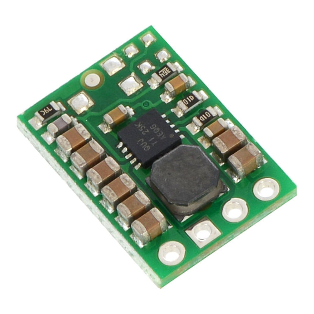
Pololu 3.3V Step-Up/Step-Down Voltage Regulator S7V8F3
Price:
Sale price
£9.60
Stock:
Quantity:
Login / Signup
Cart
Your cart is empty


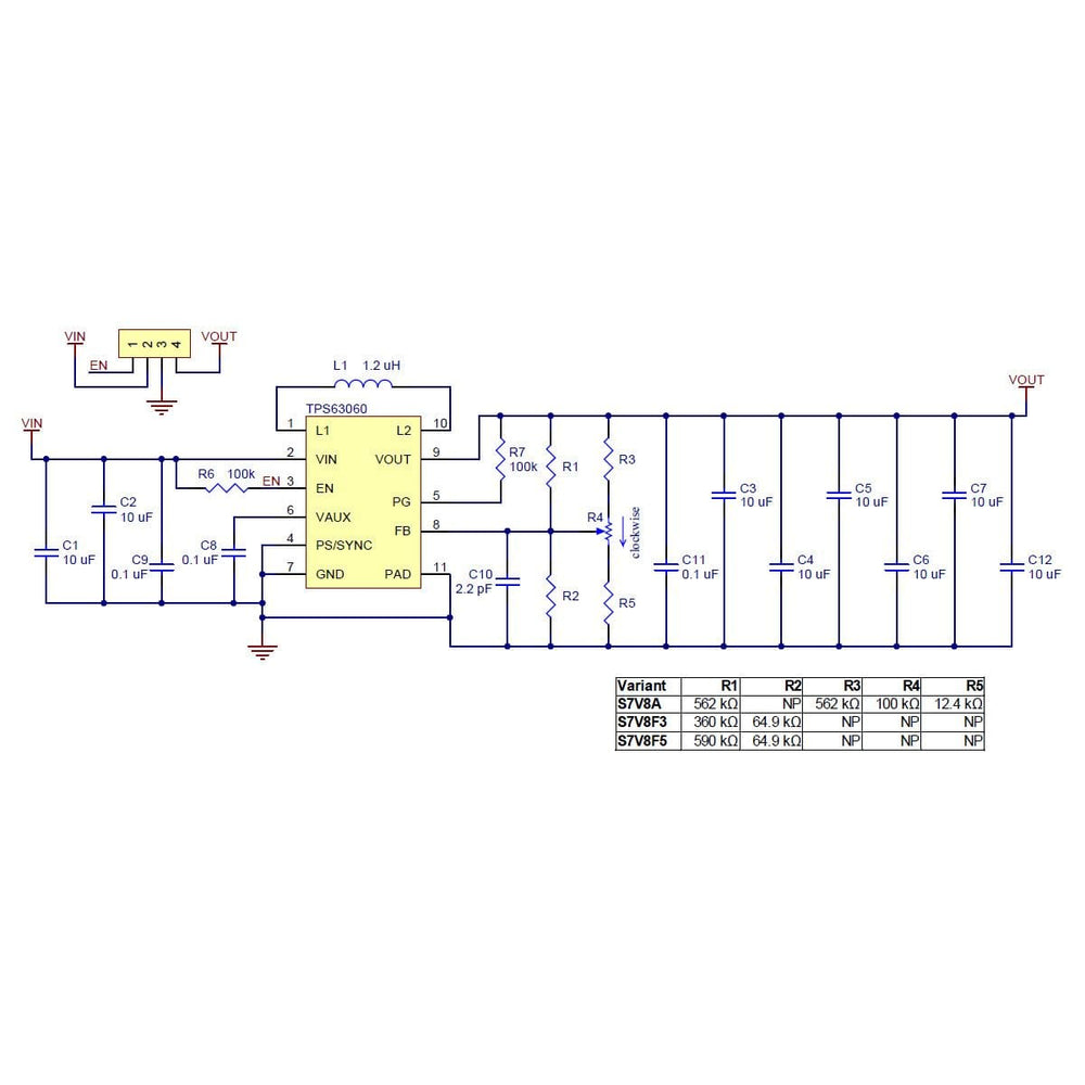
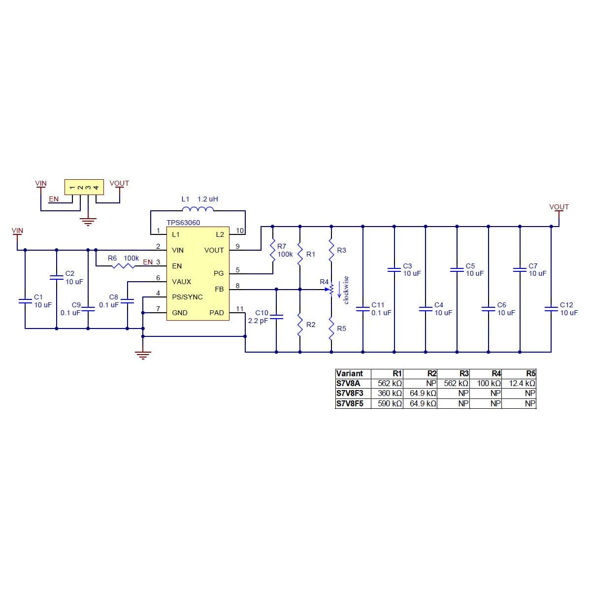
The Pololu step-up/step-down voltage regulator S7V8F3 is a switching regulator (also called a switched-mode power supply (SMPS) or DC-to-DC converter) that uses a buck-boost topology.
It takes an input voltage from 2.7V to 11.8V and increases or decreases the voltage to a fixed 3.3V output with a typical efficiency of over 90%. The input voltage can be higher than, lower than, or equal to the set output voltage, and the voltage is regulated to achieve a steady 3.3V.
During normal operation, this product can get hot enough to burn you. Take care when handling this product or other components connected to it.
This flexibility in input voltage is especially well-suited for battery-powered applications in which the battery voltage begins above the desired output voltage and drops below the target as the battery discharges. Without the typical restriction on the battery voltage staying above the required voltage throughout its life, new battery packs and form factors can be considered. For example:
In typical applications, this regulator can deliver up to 1 A continuous when the input voltage is higher than 3.3 V (stepping down). When the input voltage is lower than 3.3 V (stepping up), the available current decreases as the difference between the voltages increases; please see the graphs at the bottom of this page for more detailed characterization. The regulator has short-circuit protection, and thermal shutdown prevents damage from overheating; the board does not have reverse-voltage protection.
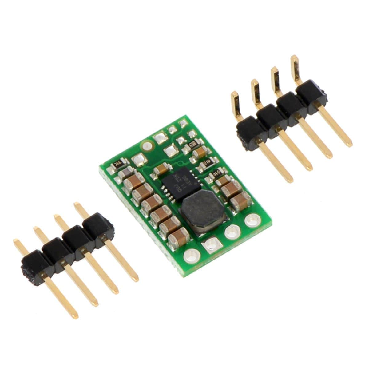
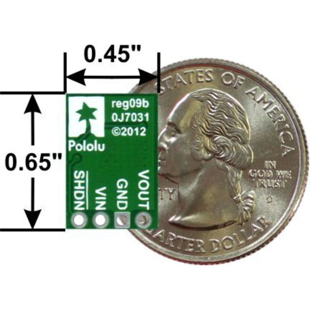
The step-up/step-down regulator has four connections: shutdown (SHDN), input voltage (VIN), ground (GND), and output voltage (VOUT).
The SHDN pin can be driven low (under 0.4 V) to power down the regulator and put it in a low-power state. The quiescent current in this sleep mode is dominated by the current in the 100k pull-up resistor from SHDN to VIN. With SHDN held low, this resistor will draw 10 µA per volt on VIN (for example, the sleep current with a 5 V input will be 50 µA). The SHDN pin can be driven high (above 1.2 V) to enable the board, or it can be connected to VIN or left disconnected if you want to leave the board permanently enabled.
The input voltage, VIN, should be between 2.7 V and 11.8 V. Lower inputs can shut down the voltage regulator; higher inputs can destroy the regulator, so you should ensure that noise on your input is not excessive, and you should be wary of destructive LC spikes (see below for more information).
The output voltage, VOUT, is fixed at 3.3 V. The output voltage can be up to 3% higher than normal when there is little or no load on the regulator. The output voltage can also drop depending on the current draw, especially when the regulator is boosting from a lower voltage (stepping up), although it should remain within 5% of the set output.
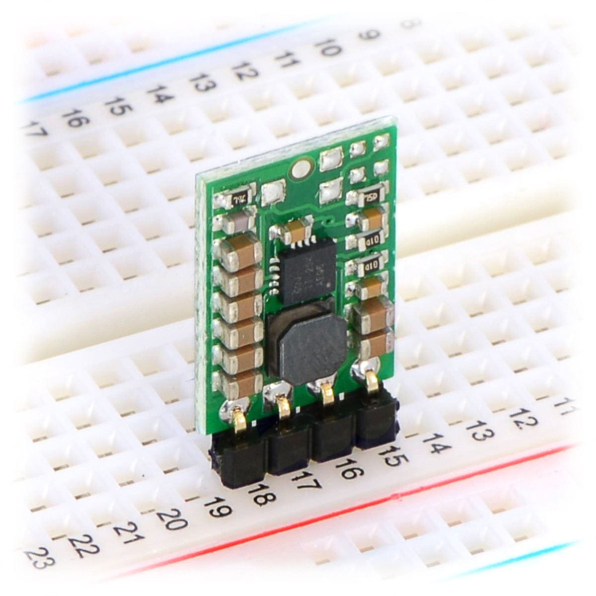
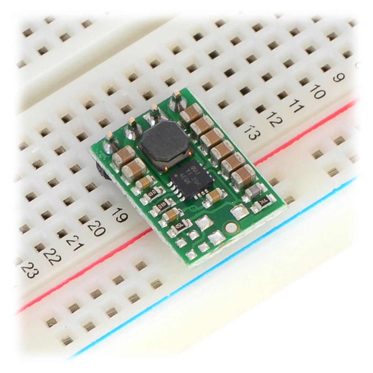
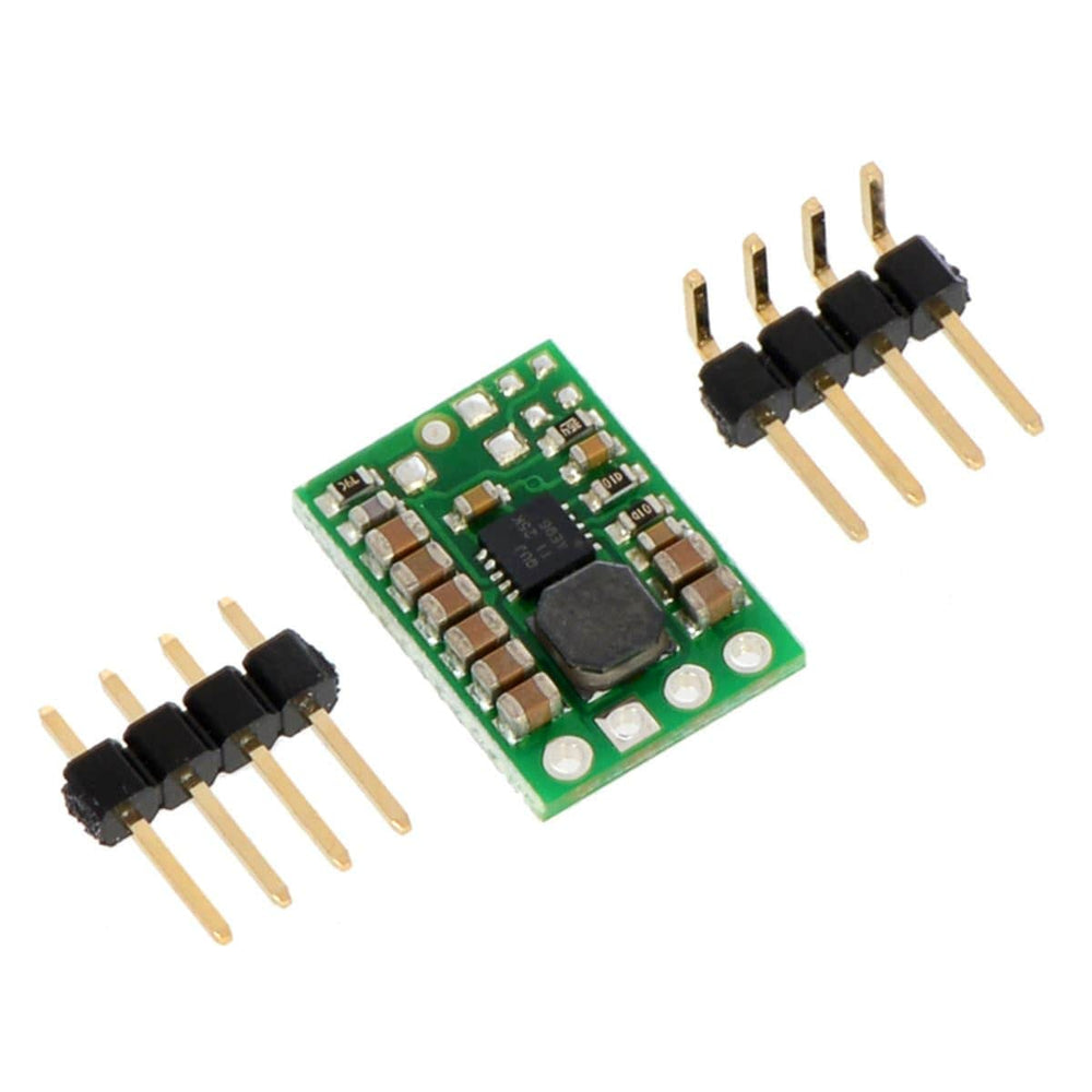
The four connections are labelled on the backside of the PCB, and they are arranged with a 0.1″ spacing along the edge of the board for compatibility with standard solderless breadboards and perfboards and connectors that use a 0.1″ grid. You can solder wires directly to the board or solder in either the 4×1 straight male header strip or the 4×1 right-angle male header strip that is included.
The efficiency of a voltage regulator, defined as (Power out)/(Power in), is an important measure of its performance, especially when battery life or heat are concerns. As shown in the graph below, this switching regulator has an efficiency of between 80% to 95% for most applications. A power-saving feature maintains these high efficiencies even when the regulator current is very low.

The maximum achievable output current of the board varies with the input voltage but also depends on other factors, including the ambient temperature, air flow, and heat sinking.
The graph below shows output currents at which this voltage regulator’s over-temperature protection typically kicks in after a few seconds. These currents represent the limit of the regulator’s capability and cannot be sustained for long periods, so the continuous currents that the regulator can provide are typically several hundred milliamps lower, and we recommend trying to draw no more than about 1 A from this regulator throughout its input voltage range.

When connecting voltage to electronic circuits, the initial rush of current can cause voltage spikes that are much higher than the input voltage. If these spikes exceed the regulator’s maximum voltage, the regulator can be destroyed. If you are connecting more than about 9 V, using power leads more than a few inches long, or using a power supply with high inductance, we recommend soldering a 33 μF or larger electrolytic capacitor close to the regulator between VIN and GND. The capacitor should be rated for at least 16 V.
| Minimum operating voltage | 2.7 V |
| Maximum operating voltage | 11.8 V |
| Maximum output current | 1A |
| Output voltage | 3.3 V |
| Reverse voltage protection? | N |
| Maximum quiescent current | 0.1 mA |
| Size | 0.45″ × 0.65″ × 0.1″ |
| Weight | 0.6 g |
Your payment information is processed securely. We do not store credit card details nor have access to your credit card information.