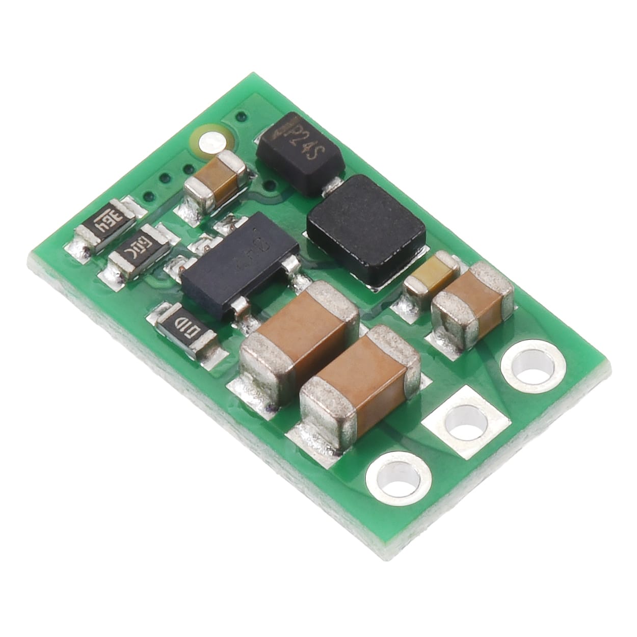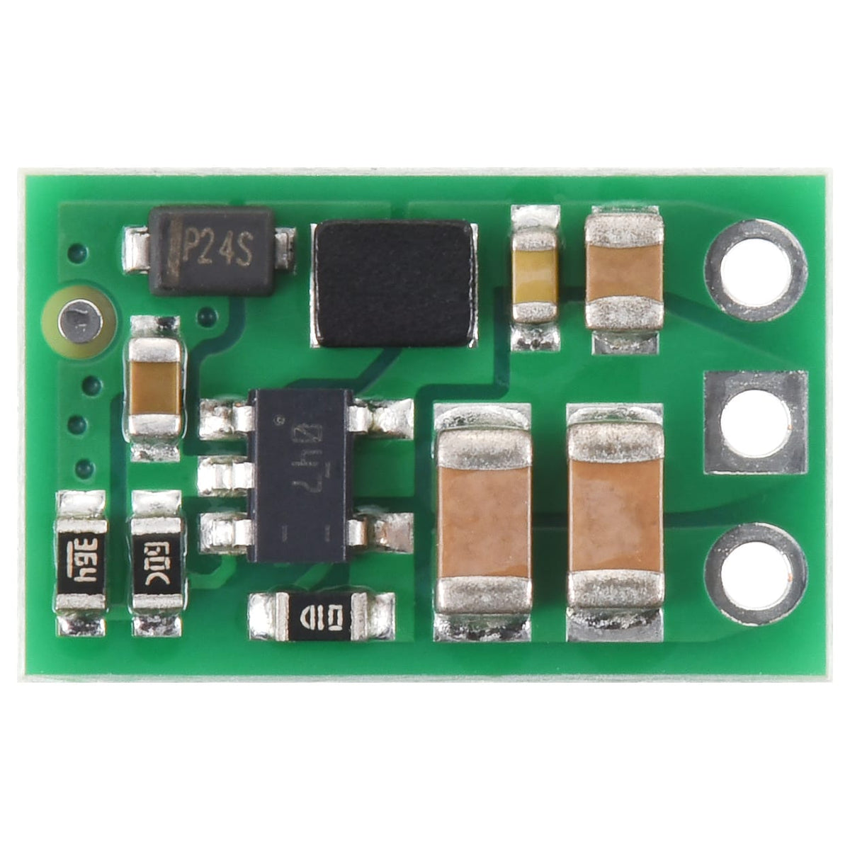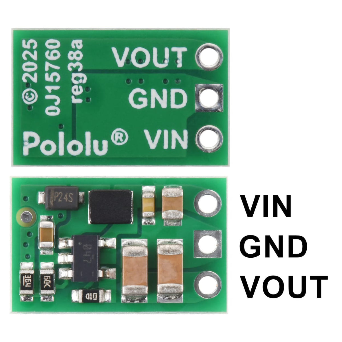
Pololu 12V Step-Up Voltage Regulator U3V9F12
Price:
Sale price
£3.40
Stock:
Quantity:
Login / Signup
Cart
Your cart is empty


The Pololu 12V Step-Up Voltage Regulator U3V9F12 generates a 12V output voltage from input voltage as low as 2.6V. They are switching regulators (also called switched-mode power supplies (SMPS) or DC-to-DC converters) and have typical efficiencies between 75% and 95%.
The regulators actively limit the instantaneous input currents to 2.2A when boosting, and input currents up to around 900mA can typically be maintained for many minutes without triggering thermal shutdown, though the actual performance depends on the input and output voltages as well as external factors such as ambient temperature and airflow.
For boost regulators, the output current equals the input current times the efficiency divided by the boost ratio of VOUT to VIN, so the more you are boosting, the lower the maximum output current will be (see the maximum continuous output current section below for performance graphs).
These regulators have several built-in protections, including cycle-by-cycle input current limiting and over-temperature shutdown.
Warning: During normal operation, this product can get hot enough to burn you. Take care when handling this product or other components connected to it.
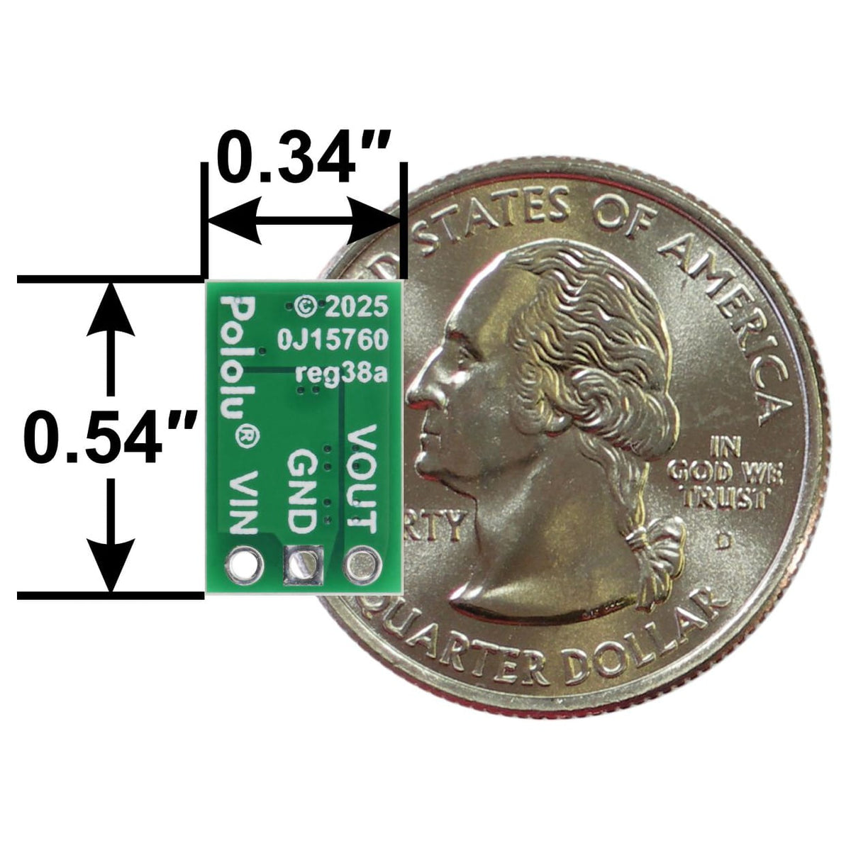
| Size | 13.6 × 8.6 × 2.8 mm |
| Weight | 0.4 g |
| Minimum operating voltage | 2.6V |
| Maximum operating voltage | 20V1 |
| Maximum input current | 2.2A2 |
| Output voltage | 12V |
| Reverse voltage protection? | N |
| Maximum quiescent current | 3mA3 |
| PCB dev codes | reg38a |
| Other PCB markings | 0J15760 |
1 - The input voltage is passed through to the output of the regulator if VIN exceeds VOUT.
2 - Instantaneous. This is the rating for the switch, and the regulator actively limits input current to this when boosting. Sustainable input current is closer to 900 mA and depends on input and output voltage and external conditions like ambient temperature and airflow. See the graph under the description tab for more information.
3 - See the quiescent current graph under the description tab for more information.

The input voltage, VIN, must be at least 2.6V and should not exceed 20V. Please note that if VIN is higher than VOUT, the higher input voltage will show up on the output, which could be dangerous for your connected load if it cannot tolerate that higher voltage. The regulator itself should generally be able to tolerate such pass-through voltages as long as they do not exceed 20V and the load is not trying to draw currents through the regulator that are beyond what the regulator can withstand.
VOUT is the regulated output voltage. The regulator’s soft-start feature gradually ramps up the VOUT voltage on start-up to limit in-rush current draw. The U3V9Fx regulators do not have short-circuit protection, so they could be damaged if exposed to output shorts or excessive loads, and they do not have reverse-voltage protection. Reverse-voltage protection modules are available separately that can be inserted between the power supply and these regulators to protect them from accidental reversal of input power polarity.
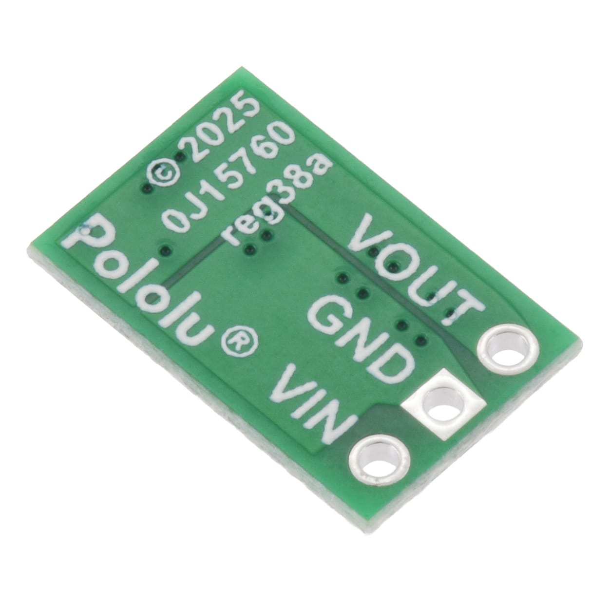
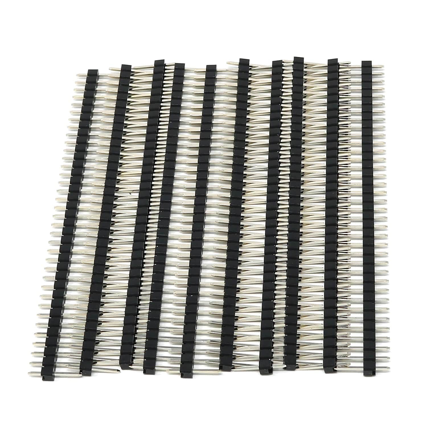
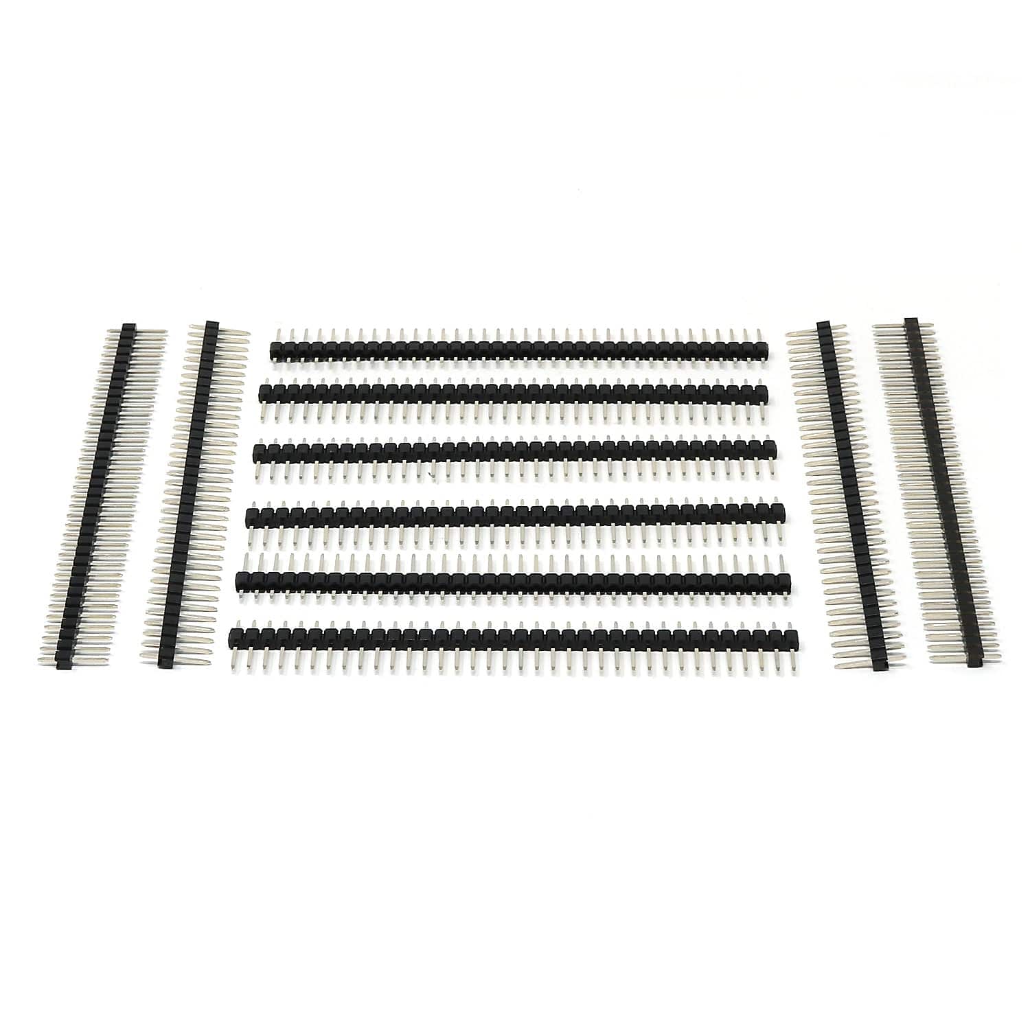
The connections are labeled on the back side of the PCB and are arranged with a 0.1″ spacing along the edge of the board for compatibility with solderless breadboards, connectors, and other prototyping arrangements that use a 0.1″ grid. You can solder wires or 0.1″ headers directly to the board. Note: header pins are not included with this product, but 1×3 straight male headers and 1×3 right-angle male headers are available separately.
The efficiency of a voltage regulator, defined as (Power out)/(Power in), is an important measure of its performance, especially when battery life or heat are concerns.

The maximum achievable output current is approximately proportional to the ratio of the input voltage to the output voltage. Additionally, the maximum output current can depend on other factors, including the ambient temperature and air flow. The graph below shows the typical maximum continuous output currents these regulators can deliver at room temperature with no forced airflow or heat sinking.
Warning: During normal operation, this product can get hot enough to burn you. Take care when handling this product or other components connected to it.

The quiescent current is the current the regulator uses just to power itself, and the graph below shows this for the different regulator versions as a function of the input voltage.

When connecting voltage to electronic circuits, the initial rush of current can cause damaging voltage spikes that are much higher than the input voltage.
In our tests with this family of regulator connected with typical power leads (~30″ test clips), we found that input voltages up to 13 V did not generally cause spikes high enough to damage the regulator itself, but even lower input voltages did cause spikes that could still be problematic for boost regulators operating with the input voltage close to the set output voltage, since input voltages above the set output voltage will propagate to the output and could damage circuits being powered by the regulator.
An electrolytic capacitor (33 μF is a good starting point) can be added close to the regulator between VIN and GND to help suppress these spikes.
More information about LC spikes can be found in our application note, Understanding Destructive LC Voltage Spikes.
Your payment information is processed securely. We do not store credit card details nor have access to your credit card information.