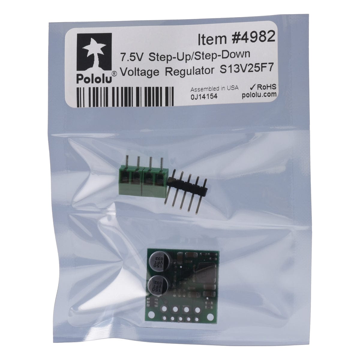
Pololu 7.5V 2.5A Step-Up/Step-Down Voltage Regulator S13V25F7
Price:
Sale price
£13.20
Stock:
Quantity:
 Skip to content
Cart
Your cart is empty


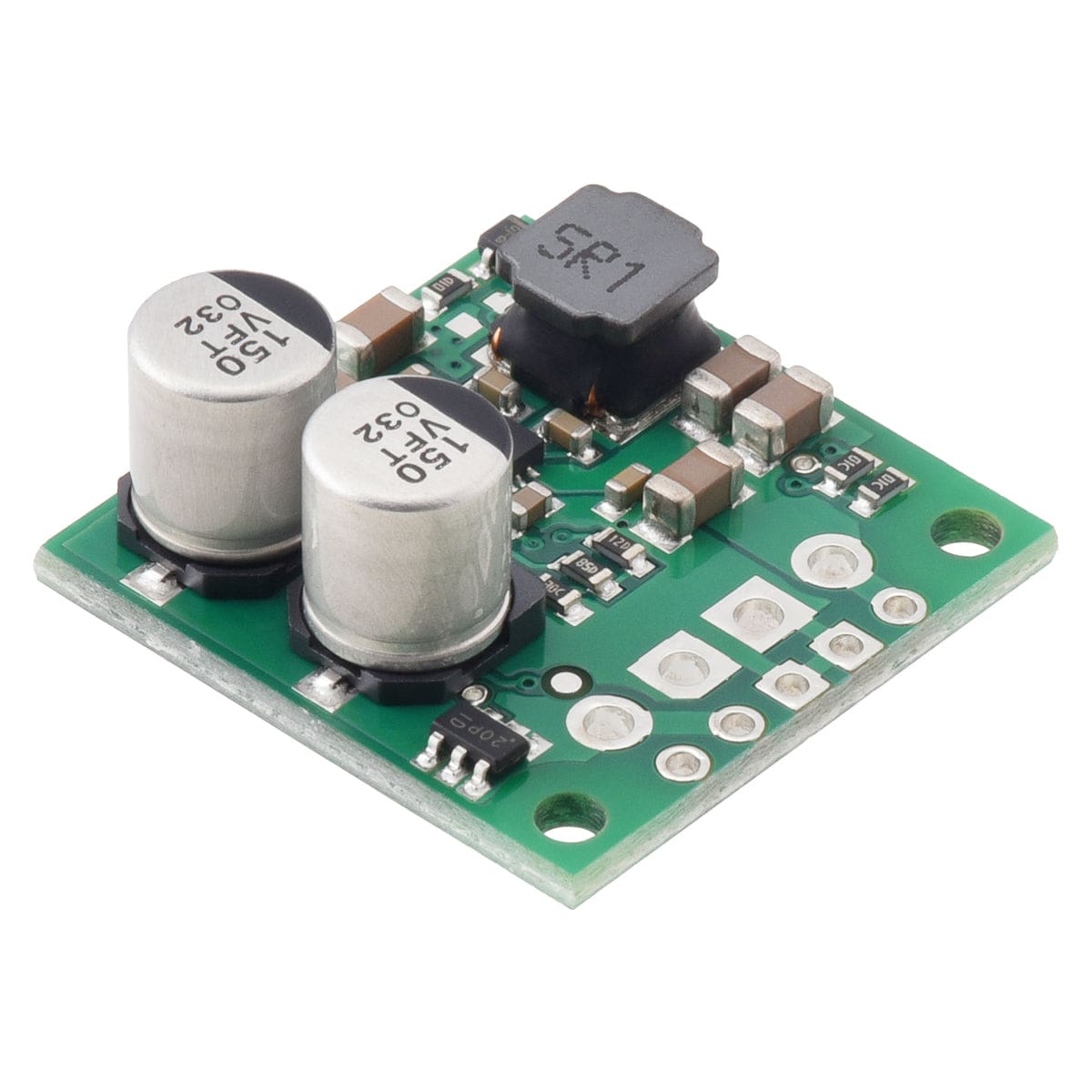
This synchronous switching step-up/step-down regulator from Pololu efficiently produces 7.5V from input voltages between 2.8 V and 22 V.
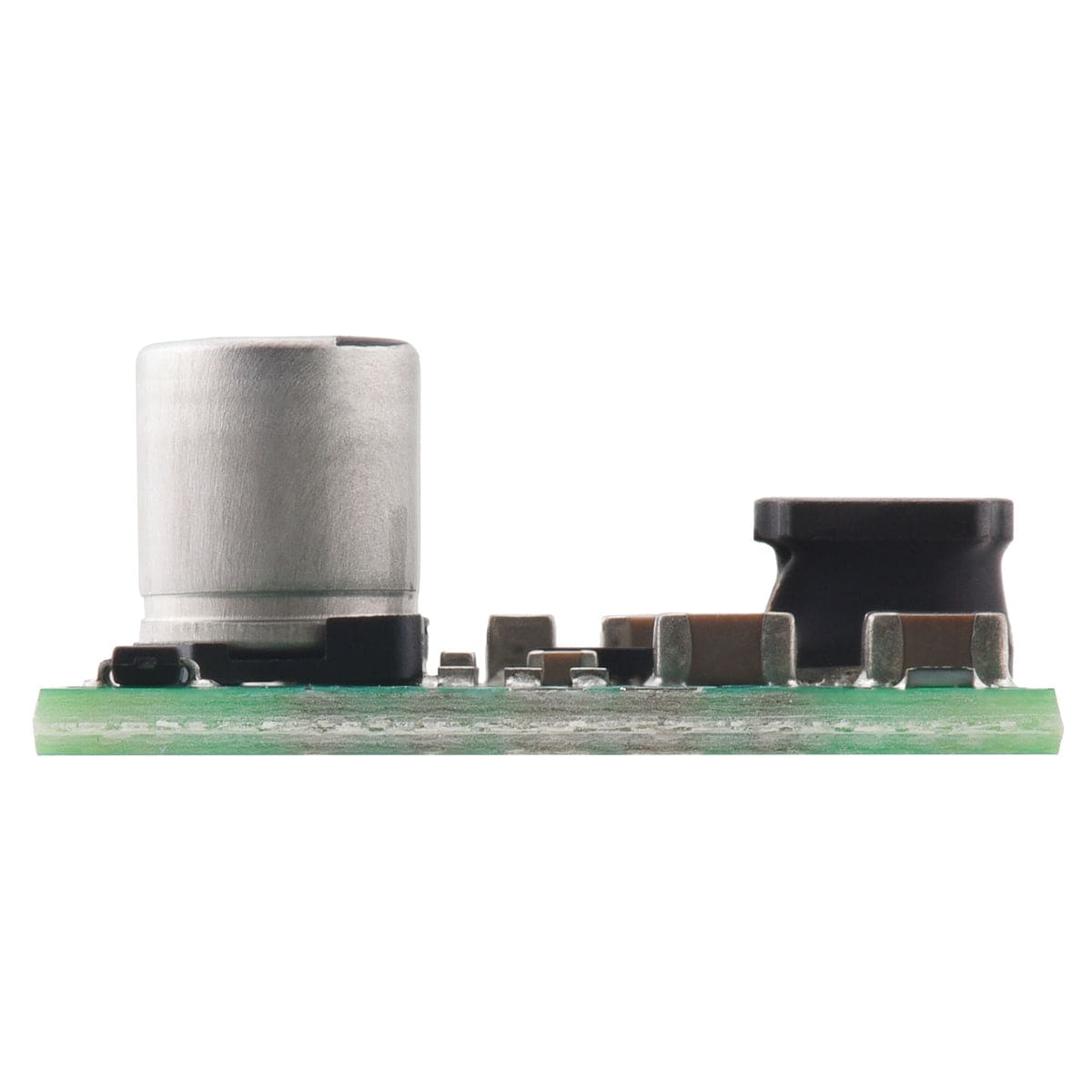
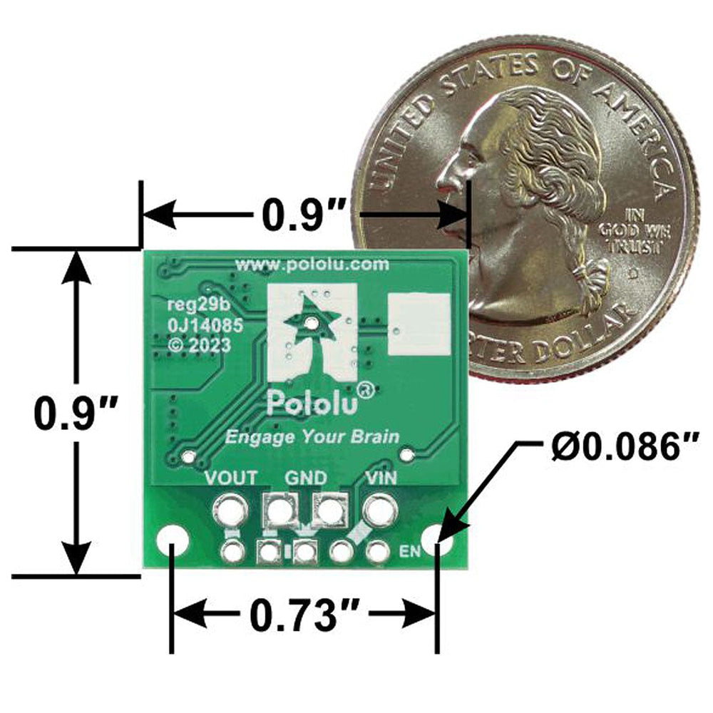
Its ability to convert both higher and lower input voltages makes it useful for applications where the power supply voltage can vary greatly, as with batteries that start above but discharge below 7.5V. The board measures 0.9″ × 0.9″, has a typical efficiency of 85% to 95%, and can supply typical continuous output currents between 1A and 3.5A depending on the input voltage. The regulator also features reverse voltage protection and an optional enable input that can be used to put the regulator in a low-power state with a current draw of less than 10 µA per volt on VIN.
Warning: During normal operation, this product can get hot enough to burn you. Take care when handling this product or other components connected to it.
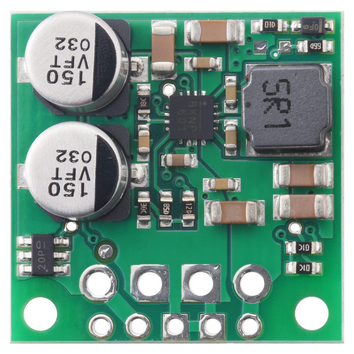
The S13V25Fx family of efficient switching regulators (also called switched-mode power supplies (SMPS) or DC-to-DC converters) use a buck-boost topology to convert both higher and lower input voltages to a regulated output voltage. They take input voltages from 2.8 V to 22 V and increase or decrease them as necessary, offering a typical efficiency of over 85% and typical continuous output currents between 1 A and 3 A.
The flexibility in input voltage offered by this family of regulators is especially well-suited for battery-powered applications in which the battery voltage begins above the regulated voltage and drops below as the battery discharges. Without the typical restriction on the battery voltage staying above the required voltage throughout its life, new battery packs and form factors can be considered.
The S13V25Fx regulators have under-voltage lockout, output over-voltage protection, over-current protection, and reverse-voltage protection up to 20 V. A thermal shutdown feature also helps prevent damage from overheating and a soft-start feature limits the inrush current and gradually ramps the output voltage on startup.
This family consists of six 2.5 A regulators with output voltages ranging from 3.3 V to 15 V. These all use the same PCB with different components populated to achieve the different output voltages:
The different versions of the S13V25Fx regulators all look very similar, so the bottom silkscreen includes a blank space where you can add your own distinguishing marks or labels.
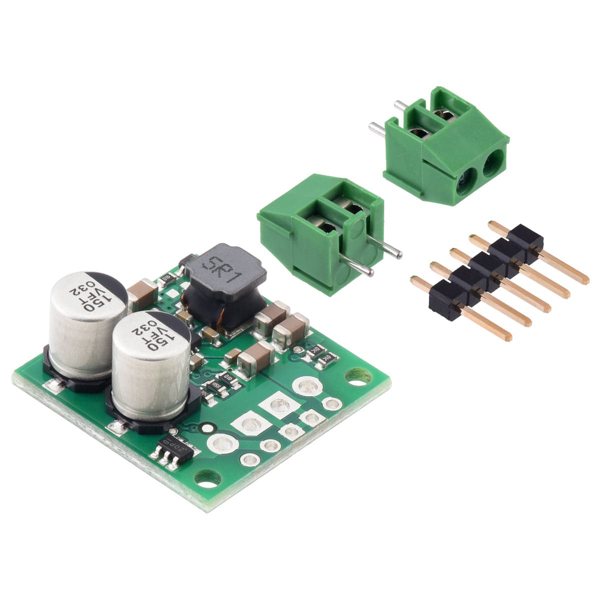
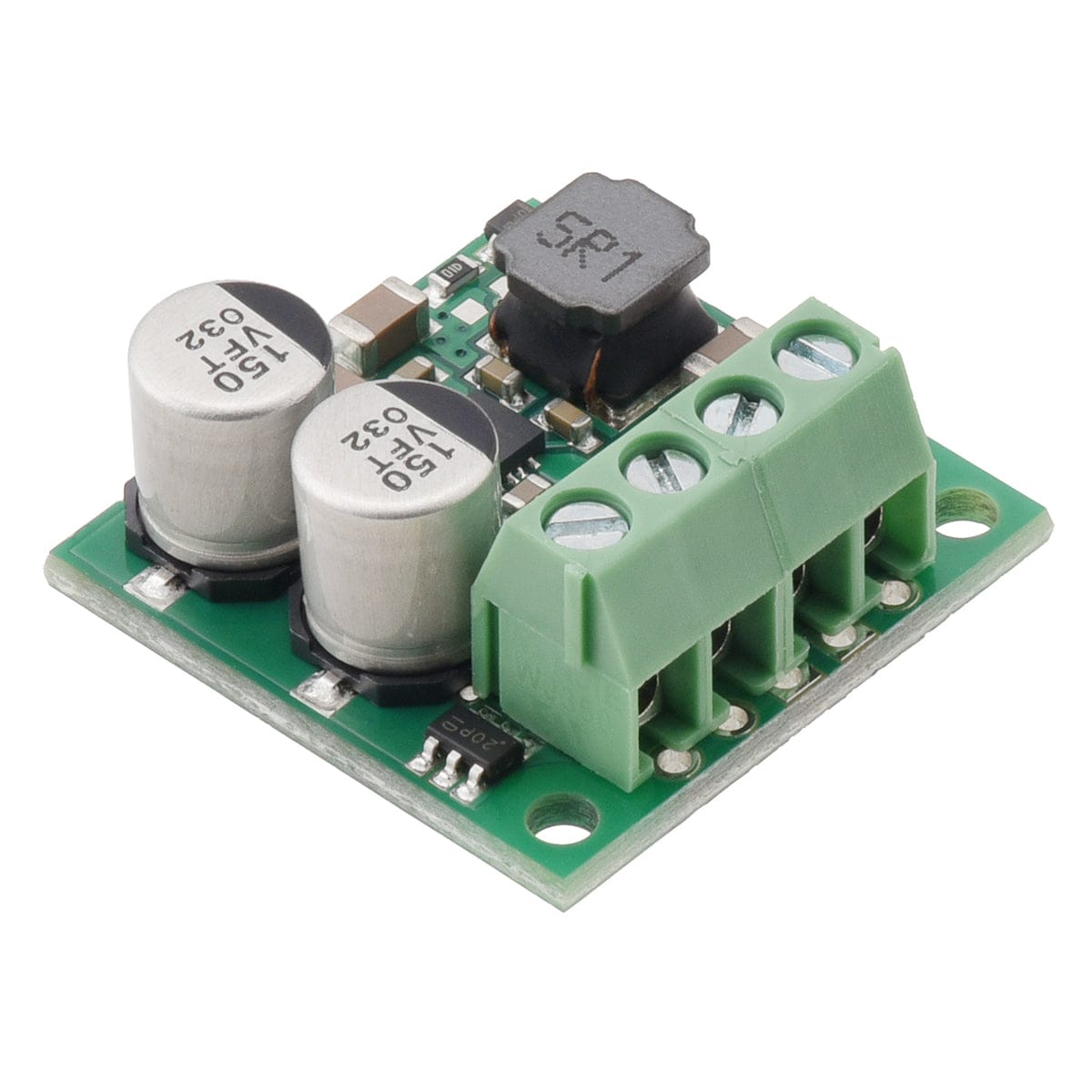
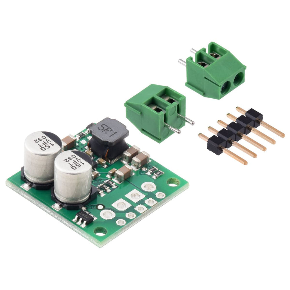
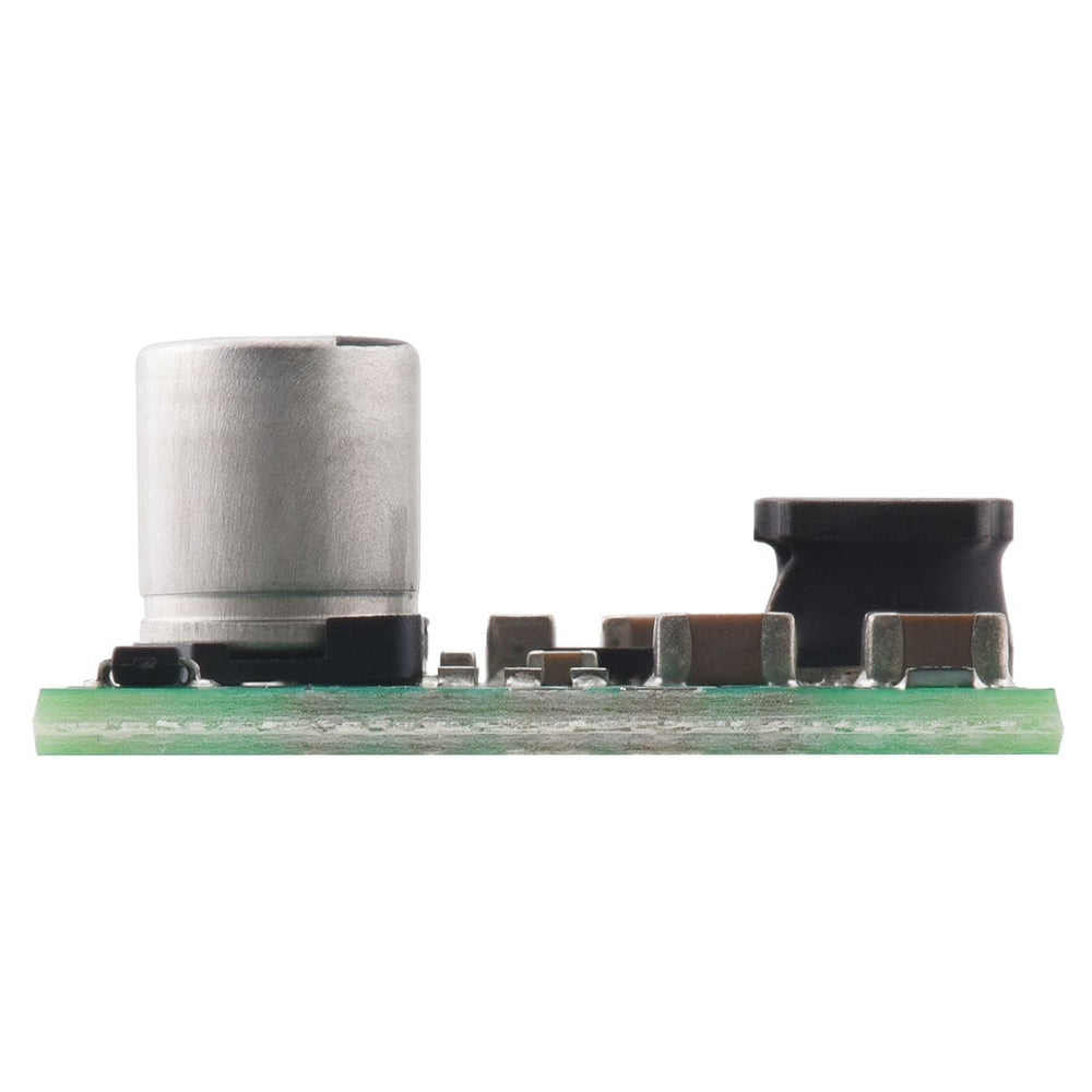
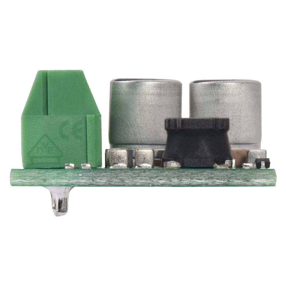
The regulator includes a 5×1 straight male header strip and two 2-pin, 3.5 mm-pitch terminal blocks, and it can be assembled with either the header or terminal blocks, not both.
The 0.1″ male header can be soldered into the smaller through-holes. Alternatively, the terminal blocks can be locked together and soldered into the larger holes to allow for convenient temporary connections of unterminated wires (see our short video on terminal block installation). You can also solder wires directly to the board for the most compact installation:

If the terminal blocks are used, a small wire (not included) can be soldered to the enable pin as shown below, so it will not interfere with the VIN terminal block connection.


The step-up/step-down regulator has four connections: enable (EN), the input voltage (VIN), ground (GND), and the output voltage (VOUT). The input voltage, VIN, powers the regulator. Voltages between 2.8 V and 22 V can be applied to VIN. VOUT is the regulated output voltage.
The regulator, which is enabled by default, can be put into a low-power sleep state by bringing the EN pin low. The rising threshold for the EN pin is between 1 V and 1.2 V, and the typical falling threshold is 100 mV lower than that (i.e. the typical falling hysteresis is 100 mV). This allows a precise low-VIN cutoff to be set, such as with the output of an external voltage divider powered by VIN, which can be useful for battery-powered applications where draining the battery below a particular voltage threshold could permanently damage it. The quiescent current draw in sleep mode is dominated by the current in the 475 kΩ pull-up resistor from ENABLE to VIN and in the reverse-voltage protection circuit, which altogether will be between 2 µA and 10 µA per volt on VIN.
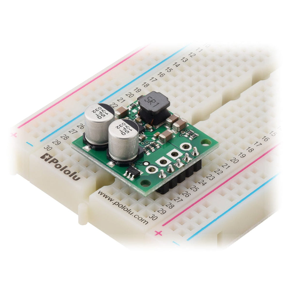
The regulator has two sets of through-holes: five smaller holes arranged with a 0.1″ spacing along the edge of the board (for compatibility with standard solderless breadboards and perfboards and connectors that use a 0.1″ grid) and four larger holes intended for 3.5 mm-pitch terminal blocks. VIN, GND, and VOUT are available at both the smaller holes and larger holes, but EN is only available on the smaller row of through holes.
The efficiency of this specific voltage regulator, defined as (Power out)/(Power in), is an important measure of its performance, especially when battery life or heat are concerns.

The maximum achievable output current of the regulator varies with the input voltage but also depends on other factors, including the ambient temperature, air flow, and heat sinking. The graph below shows the maximum output currents that the regulators in the S13V25Fx family can deliver continuously at room temperature in still air and without additional heat sinking.

The quiescent current is the current the regulator uses just to power itself, and the graph below shows this as a function of the input voltage. The module’s EN input can be driven low to put the board into a low-power state where it typically draws between 2 µA and 10 µA per volt on VIN.

| Minimum operating voltage | 2.8 V |
| Maximum operating voltage | 22 V |
| Continuous output current | 2.5 A |
| Output voltage | 7.5 V |
| Reverse voltage protection? | Y |
| Maximum quiescent current | 25 mA |
| Output type | Fixed 7.5V |
| Size | 0.9″ × 0.9″ × 0.38″ |
| Weight | 3.8 g |
Your payment information is processed securely. We do not store credit card details nor have access to your credit card information.